ZHCSC62D March 2014 – December 2017 UCC28630 , UCC28631 , UCC28632 , UCC28633 , UCC28634
PRODUCTION DATA.
- 1 特性
- 2 应用
- 3 说明
- 4 修订历史记录
- 5 Device Comparison Table
- 6 Pin Configuration and Functions
- 7 Specifications
-
8 Detailed Description
- 8.1 Overview
- 8.2 Functional Block Diagram
- 8.3
Feature Description
- 8.3.1 High-Voltage Current Source Start-Up Operation
- 8.3.2 AC Input UVLO / Brownout Protection
- 8.3.3 Active X-Capacitor Discharge (UCC28630 and UCC28633 only)
- 8.3.4 Magnetic Input and Output Voltage Sensing
- 8.3.5 Fixed-Point Magnetic Sense Sampling Error Sources
- 8.3.6 Magnetic Sense Resistor Network Calculations
- 8.3.7 Magnetic Sensing: Power Stage Design Constraints
- 8.3.8 Magnetic Sense Voltage Control Loop
- 8.3.9 Peak Current Mode Control
- 8.3.10 IPEAK Adjust vs. Line
- 8.3.11 Primary-Side Constant-Current Limit (CC Mode)
- 8.3.12 Primary-Side Overload Timer (UCC28630 only)
- 8.3.13 Overload Timer Adjustment (UCC28630 only)
- 8.3.14 CC-Mode IOUT(lim) Adjustment
- 8.3.15 Fault Protections
- 8.3.16 Pin-Fault Detection and Protection
- 8.3.17 Over-Temperature Protection
- 8.3.18 External Fault Input
- 8.3.19 External SD Pin Wake Input (except UCC28633)
- 8.3.20 External Wake Input at VSENSE Pin (UCC28633 Only)
- 8.3.21 Mode Control and Switching Frequency Modulation
- 8.3.22 Frequency Dither For EMI (except UCC28632)
- 8.4 Device Functional Modes
-
9 Applications and Implementation
- 9.1 Application Information
- 9.2
Typical Application
- 9.2.1 Notebook Adapter, 19.5 V, 65 W
- 9.2.2 UCC28630 Application Schematic
- 9.2.3 Design Requirements
- 9.2.4
Detailed Design Procedure
- 9.2.4.1 Custom Design With WEBENCH® Tools
- 9.2.4.2 Input Bulk Capacitance and Minimum Bulk Voltage
- 9.2.4.3 Transformer Turn Ratio
- 9.2.4.4 Transformer Magnetizing Inductance
- 9.2.4.5 Current Sense Resistor RCS
- 9.2.4.6 Transformer Constraint Verification
- 9.2.4.7 Transformer Selection and Design
- 9.2.4.8 Slope Compensation Verification
- 9.2.4.9 Power MOSFET and Output Rectifier Selection
- 9.2.4.10 Output Capacitor Selection
- 9.2.4.11 Calculation of CC Mode Limit Point
- 9.2.4.12 VDD Capacitor Selection
- 9.2.4.13 Magnetic Sense Resistor Network Selection
- 9.2.4.14 Output LED Pre-Load Resistor Calculation
- 9.2.5 External Wake Pulse Calculation at VSENSE Pin (UCC28633 Only)
- 9.2.6 Energy Star Average Efficiency and Standby Power
- 9.2.7 Application Performance Plots
- 9.3 Dos and Don'ts
- 10Power Supply Recommendations
- 11Layout
- 12器件和文档支持
- 13机械、封装和可订购信息
8.3.13 Overload Timer Adjustment (UCC28630 only)
The UCC28630 overload timer trip level and time constant are both selectable from a defined list of combinations. The user can select the overload timer trip level as a percentage of the rated continuous nominal power, PNOM (see Figure 41), and the timer response speed. The available choices are detailed in Table 2.
Table 2. Overload Timer Adjustment
| RPROG PROGRAMMING RESISTOR (kΩ) (E96 series values) | TIMER CONTINUOUS OPERATION PTRIP/PNOM (%) | TIME CONSTANT AT 200% of PNOM OR IN CC MODE (ms) |
|---|---|---|
| Open, or > 47 | 160 | 1000 |
| 20.0 | 160 | 500 |
| 12.7 | 160 | 150 |
| 9.31 | 135 | 1000 |
| 7.32 | 135 | 500 |
| 6.04 | 135 | 150 |
| 5.11 | 110 | 1000 |
| 4.42 | 110 | 500 |
| 3.92 | 110 | 150 |
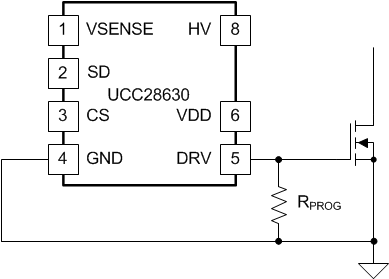
The desired pull-down resistance on the DRV pin sets the required overload parameters, as shown in Figure 36. The controller measures the resistance value on the DRV pin at start-up using a low-level test voltage (400 mV to ensure it is well below the lowest possible power MOSFET gate threshold voltage) and sensing the current that flows. Thus, based on the resistance RPROG, the required set of timer parameters can be chosen.
 Figure 36. Overload Timer Setting Adjustment
 (with programming pull-down resistor on DRV pin)
To ensure that the sensed current does not sit close to an interval boundary, the resistor values listed in Table 2 (or the closest value possible) should be used. These recommended resistor values position the test current in the center of each interval.