ZHCSC62D March 2014 – December 2017 UCC28630 , UCC28631 , UCC28632 , UCC28633 , UCC28634
PRODUCTION DATA.
- 1 特性
- 2 应用
- 3 说明
- 4 修订历史记录
- 5 Device Comparison Table
- 6 Pin Configuration and Functions
- 7 Specifications
-
8 Detailed Description
- 8.1 Overview
- 8.2 Functional Block Diagram
- 8.3
Feature Description
- 8.3.1 High-Voltage Current Source Start-Up Operation
- 8.3.2 AC Input UVLO / Brownout Protection
- 8.3.3 Active X-Capacitor Discharge (UCC28630 and UCC28633 only)
- 8.3.4 Magnetic Input and Output Voltage Sensing
- 8.3.5 Fixed-Point Magnetic Sense Sampling Error Sources
- 8.3.6 Magnetic Sense Resistor Network Calculations
- 8.3.7 Magnetic Sensing: Power Stage Design Constraints
- 8.3.8 Magnetic Sense Voltage Control Loop
- 8.3.9 Peak Current Mode Control
- 8.3.10 IPEAK Adjust vs. Line
- 8.3.11 Primary-Side Constant-Current Limit (CC Mode)
- 8.3.12 Primary-Side Overload Timer (UCC28630 only)
- 8.3.13 Overload Timer Adjustment (UCC28630 only)
- 8.3.14 CC-Mode IOUT(lim) Adjustment
- 8.3.15 Fault Protections
- 8.3.16 Pin-Fault Detection and Protection
- 8.3.17 Over-Temperature Protection
- 8.3.18 External Fault Input
- 8.3.19 External SD Pin Wake Input (except UCC28633)
- 8.3.20 External Wake Input at VSENSE Pin (UCC28633 Only)
- 8.3.21 Mode Control and Switching Frequency Modulation
- 8.3.22 Frequency Dither For EMI (except UCC28632)
- 8.4 Device Functional Modes
-
9 Applications and Implementation
- 9.1 Application Information
- 9.2
Typical Application
- 9.2.1 Notebook Adapter, 19.5 V, 65 W
- 9.2.2 UCC28630 Application Schematic
- 9.2.3 Design Requirements
- 9.2.4
Detailed Design Procedure
- 9.2.4.1 Custom Design With WEBENCH® Tools
- 9.2.4.2 Input Bulk Capacitance and Minimum Bulk Voltage
- 9.2.4.3 Transformer Turn Ratio
- 9.2.4.4 Transformer Magnetizing Inductance
- 9.2.4.5 Current Sense Resistor RCS
- 9.2.4.6 Transformer Constraint Verification
- 9.2.4.7 Transformer Selection and Design
- 9.2.4.8 Slope Compensation Verification
- 9.2.4.9 Power MOSFET and Output Rectifier Selection
- 9.2.4.10 Output Capacitor Selection
- 9.2.4.11 Calculation of CC Mode Limit Point
- 9.2.4.12 VDD Capacitor Selection
- 9.2.4.13 Magnetic Sense Resistor Network Selection
- 9.2.4.14 Output LED Pre-Load Resistor Calculation
- 9.2.5 External Wake Pulse Calculation at VSENSE Pin (UCC28633 Only)
- 9.2.6 Energy Star Average Efficiency and Standby Power
- 9.2.7 Application Performance Plots
- 9.3 Dos and Don'ts
- 10Power Supply Recommendations
- 11Layout
- 12器件和文档支持
- 13机械、封装和可订购信息
8.3.12 Primary-Side Overload Timer (UCC28630 only)
The internal overload timer in the UCC28630 uses the same output load current measurement that is used by the CC loop. This measurement tracks the power stage thermal stress, and protects the power stage against output overload. If the output is overloaded for too long such that the power stage would be over-stressed, then the PWM shuts down, and enters low-power mode for a time period of tRESET(long); thereafter the device discharges VDD to the VDD(reset) level and initiates a hiccup mode restart.
The overload timer operates by taking an estimate of output current, squaring it (assuming the power stage losses are dominated by resistive I2 losses) to produce (K x I2OUT), where K is a scaling gain factor. The overload timer is constantly running at every load level, and accumulates at a rate dependent on the difference between (K x I2OUT) and the previous level of the timer. If (K x I2OUT) is greater than the previous timer level, the timer level continues to increase; if (K x I2OUT) is less than the previous timer level, then the timer level decreases. At any steady load, the overload timer level eventually settles at a level proportional to I2OUT. Because the overload timer level adjusts at a rate dependent on the difference between (K xI2OUT) and the previous level, the timer initially reacts faster to larger differences, but over time settles exponentially at a level proportional to (K x I2OUT).
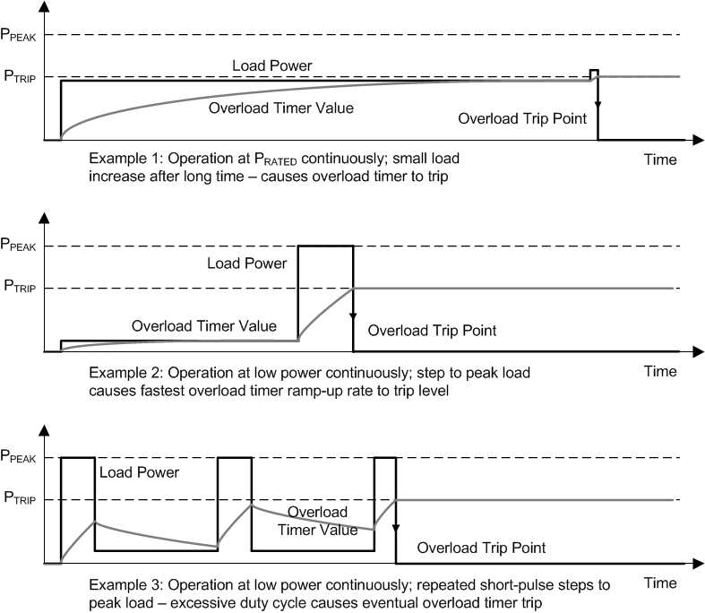
As shown in Figure 34, in both the first and second examples, the initial steady load allows the timer to integrate and settle at a level proportional to the load. The margin to the over-load trip level depends on the historical loading, lower prior average loading results in greater future over-load capability, and vice versa. The rate at which the timer reacts to different load steps is set by the chosen time constant (or response rate) per Table 2.
The overload timer can cope with pulsed loads and loads with a complex waveform. Because the rate of increase and decrease also depends on the load change from the previous load, it also times out faster for bigger overloads, or allows a smaller overload to run for much longer. The overload timer operates in both normal CV mode and overload CC mode, or a dynamic mix of both modes.
 Figure 34. Overload Timer Example Waveforms Under Various Load Scenarios
  Figure 35. Overload Timer Block Diagram