ZHCSC62D March 2014 – December 2017 UCC28630 , UCC28631 , UCC28632 , UCC28633 , UCC28634
PRODUCTION DATA.
- 1 特性
- 2 应用
- 3 说明
- 4 修订历史记录
- 5 Device Comparison Table
- 6 Pin Configuration and Functions
- 7 Specifications
-
8 Detailed Description
- 8.1 Overview
- 8.2 Functional Block Diagram
- 8.3
Feature Description
- 8.3.1 High-Voltage Current Source Start-Up Operation
- 8.3.2 AC Input UVLO / Brownout Protection
- 8.3.3 Active X-Capacitor Discharge (UCC28630 and UCC28633 only)
- 8.3.4 Magnetic Input and Output Voltage Sensing
- 8.3.5 Fixed-Point Magnetic Sense Sampling Error Sources
- 8.3.6 Magnetic Sense Resistor Network Calculations
- 8.3.7 Magnetic Sensing: Power Stage Design Constraints
- 8.3.8 Magnetic Sense Voltage Control Loop
- 8.3.9 Peak Current Mode Control
- 8.3.10 IPEAK Adjust vs. Line
- 8.3.11 Primary-Side Constant-Current Limit (CC Mode)
- 8.3.12 Primary-Side Overload Timer (UCC28630 only)
- 8.3.13 Overload Timer Adjustment (UCC28630 only)
- 8.3.14 CC-Mode IOUT(lim) Adjustment
- 8.3.15 Fault Protections
- 8.3.16 Pin-Fault Detection and Protection
- 8.3.17 Over-Temperature Protection
- 8.3.18 External Fault Input
- 8.3.19 External SD Pin Wake Input (except UCC28633)
- 8.3.20 External Wake Input at VSENSE Pin (UCC28633 Only)
- 8.3.21 Mode Control and Switching Frequency Modulation
- 8.3.22 Frequency Dither For EMI (except UCC28632)
- 8.4 Device Functional Modes
-
9 Applications and Implementation
- 9.1 Application Information
- 9.2
Typical Application
- 9.2.1 Notebook Adapter, 19.5 V, 65 W
- 9.2.2 UCC28630 Application Schematic
- 9.2.3 Design Requirements
- 9.2.4
Detailed Design Procedure
- 9.2.4.1 Custom Design With WEBENCH® Tools
- 9.2.4.2 Input Bulk Capacitance and Minimum Bulk Voltage
- 9.2.4.3 Transformer Turn Ratio
- 9.2.4.4 Transformer Magnetizing Inductance
- 9.2.4.5 Current Sense Resistor RCS
- 9.2.4.6 Transformer Constraint Verification
- 9.2.4.7 Transformer Selection and Design
- 9.2.4.8 Slope Compensation Verification
- 9.2.4.9 Power MOSFET and Output Rectifier Selection
- 9.2.4.10 Output Capacitor Selection
- 9.2.4.11 Calculation of CC Mode Limit Point
- 9.2.4.12 VDD Capacitor Selection
- 9.2.4.13 Magnetic Sense Resistor Network Selection
- 9.2.4.14 Output LED Pre-Load Resistor Calculation
- 9.2.5 External Wake Pulse Calculation at VSENSE Pin (UCC28633 Only)
- 9.2.6 Energy Star Average Efficiency and Standby Power
- 9.2.7 Application Performance Plots
- 9.3 Dos and Don'ts
- 10Power Supply Recommendations
- 11Layout
- 12器件和文档支持
- 13机械、封装和可订购信息
8.3.4 Magnetic Input and Output Voltage Sensing
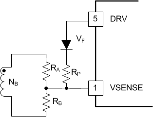
A sense winding on the transformer is used to measure the input voltage and output voltage of the power stage. This winding is typically the converter bias winding. The sense winding should be interfaced to the VSENSE pin as shown in Figure 21. This interface requires that the voltage across the winding be scaled with a resistor divider RA / RB, and then offset with a switched, pull-up resistor RP (in series with a diode) connected to the gate drive pin DRV.
 Figure 21. VSENSE Pin Interface Arrangement
 During the off-time portion of the switching cycle (also referred to as the flyback interval), the resistor divider (RB / (RA + RB)) scales the positive voltage swing at the VSENSE pin for output voltage regulation, as shown in Figure 22. During this interval, since the DRV output is low, the diode in series with RP is reverse-biased, and so RP is out-of-circuit.
 Figure 22. VOUT Sense Using the Positive Swing on the Sense Winding
 During the on-time portion of the switching cycle, when the DRV pin goes high (should swing very close to the value at the VDD pin), the switched pull-up RP allows the negative swing on the winding to be level-shifted positive, and thus also be sensed at the VSENSE pin, as shown in Figure 23. In this way the bias winding may be used to sense both line input voltage and output voltage.
NOTE
The input voltage sensed by the transformer bias winding is actually the voltage across the bulk capacitor, not the AC input voltage, because the bulk capacitor voltage appears across the primary winding when the flyback switch turns on
Uses of the sensed bulk and output voltages:
- Input AC mains UVLO
- Input brownout
- Line-dependent peak-current adjustment
- Accurate output-current regulation
- Output-voltage regulation
- Output over-voltage protection (OVP)
 Figure 23. Line Input Sense by Offsetting the Negative Swing on the Sense Winding
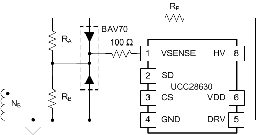
 In order to protect the VSENSE pin from excessive negative current in the event of a manufacturing fault (such as an open circuit on RP), use a series limiting resistor and clamping diode on the VSENSE pin. Combine the clamping diode and DRV pull-up diode into a single-package common-cathode diode to reduce the component count of the system. This is illustrated in Figure 24.
 Figure 24. VSENSE Pin Protection and Interface to Bias Winding
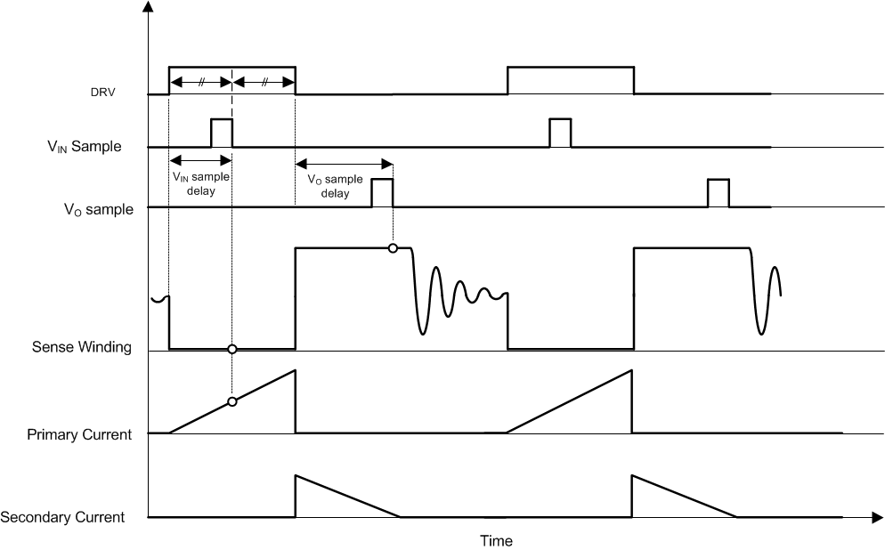
 The device continually adjusts the input voltage sample delay, measuring the sample half-way through the on-time interval, to ensure the cleanest signal. The device uses same mid-point sample trigger when measuring the main MOSFET switch current (ISW). Sampling MOSFET switch current in the middle of the on-time automatically measures the average current during the on-time, ISW(on_avg), which is required for the current limit and overload timer block.
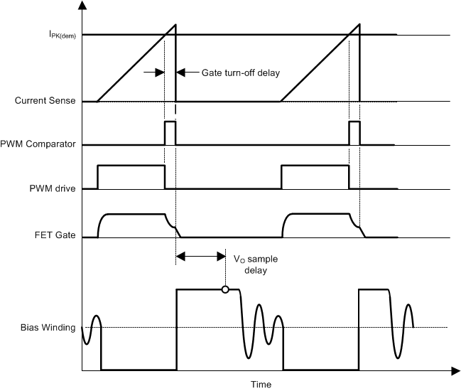
The output voltage sample point is always time relative to the turn-off instant. Internally, the device uses the CS pin to determine the cycle end, rather than the PWM falling edge on the DRV pin. The device bases this determination on the instant that the MOSFET switch current drops below the demanded peak current level (IPEAK ) at the peak current mode comparator. Some delay always occurs from the falling edge on DRV to the point when the external power MOSFET turns off. This internal timing method ensures a more accurate measure of ISW(on_avg), and also ensures that the output voltage sample point is not measured too early, before the leakage ringing has subsided. The effect of the gate turn-off delay and the adjustment of the output voltage sample point is illustrated in Figure 25.
 Figure 25. VOUT Sample Adjust for External Gate Delay
 The sampling of the input voltage and output voltage signals on the bias winding must be synchronized to the on-time and off-time flyback intervals respectively, because the signals occur during only those intervals in the switching cycle. Typical waveforms and timing are illustrated in Figure 26.
More conventional knee-point detection schemes, where the sample is measured at the end of the flyback interval when the secondary-side current has decayed to zero, inherently always operate in discontinuous conduction mode (DCM). However, the fixed sample-point scheme used on the UCC2863x has the advantages of being able to operate in regions of fixed frequency, and being able to operate in continuous conduction mode (CCM). Fixed sample-point schemes conventionally suffer poorer regulation than knee-point schemes, because there is always current flowing at the sample instant. This current produces a sensing error as a result of the voltage drop produced across the secondary-side resistance and leakage inductance. This parasitic voltage drop varies with output voltage, line and load, thus influencing the regulation. The UCC2863x devices uses a novel internal compensation scheme to adjust for this parasitic voltage drop, and can deliver excellent static line and load regulation, even when operating heavily in CCM.
 Figure 26. VIN and VOUT Sample Trigger Timing