SLUSDW0B May 2020 – May 2020 UCC28065
PRODUCTION DATA.
- 1 Features
- 2 Applications
- 3 Description
- 4 Revision History
- 5 Description (Continued)
- 6 Pin Configuration and Functions
- 7 Specifications
-
8 Detailed Description
- 8.1 Overview
- 8.2 Functional Block Diagram
- 8.3
Feature Description
- 8.3.1 Principles of Operation
- 8.3.2 Natural Interleaving
- 8.3.3 On-Time Control, Maximum Frequency Limiting, Restart Timer and Input Voltage Feed-Forward compensation
- 8.3.4 Zero-Current Detection and Valley Switching
- 8.3.5 Phase Management and Light-Load Operation
- 8.3.6 Burst Mode Operation
- 8.3.7 External Disable
- 8.3.8 Improved Error Amplifier
- 8.3.9 Soft Start
- 8.3.10 Brownout Protection
- 8.3.11 Line Dropout Detection
- 8.3.12 VREF
- 8.3.13 VCC
- 8.3.14
System Level Protections
- 8.3.14.1 Failsafe OVP - Output Over-voltage Protection
- 8.3.14.2 Overcurrent Protection
- 8.3.14.3 Open-Loop Protection
- 8.3.14.4 VCC Undervoltage Lock-Out (UVLO) Protection
- 8.3.14.5 Phase-Fail Protection
- 8.3.14.6 CS - Open, TSET - Open and Short Protection
- 8.3.14.7 Thermal Shutdown Protection
- 8.3.14.8 Fault Logic Diagram
- 8.4 Device Functional Modes
-
9 Application and Implementation
- 9.1 Application Information
- 9.2
Typical Application
- 9.2.1 Design Requirements
- 9.2.2
Detailed Design Procedure
- 9.2.2.1 Inductor Selection
- 9.2.2.2 ZCD Resistor Selection RZA, RZB
- 9.2.2.3 HVSEN
- 9.2.2.4 Output Capacitor Selection
- 9.2.2.5 Selecting RS For Peak Current Limiting
- 9.2.2.6 Power Semiconductor Selection (Q1, Q2, D1, D2)
- 9.2.2.7 Brownout Protection
- 9.2.2.8 Converter Timing
- 9.2.2.9 Programming VOUT
- 9.2.2.10 Voltage Loop Compensation
- 9.2.3 Application Curves
- 10Power Supply Recommendations
- 11Layout
- 12Device and Documentation Support
- 13Mechanical, Packaging, and Orderable Information
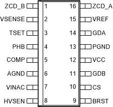
6 Pin Configuration and Functions
D Package
16-Pin SOIC
Top View

Pin Functions
| PIN | I/O | DESCRIPTION | |
|---|---|---|---|
| NAME | NO. | ||
| AGND | 6 | - | Analog ground |
| BRST | 9 | I | Burst mode threshold input |
| COMP | 5 | O | Error amplifier output |
| CS | 10 | I | Current sense input |
| GDA | 14 | O | Phase A gate driver output |
| GDB | 11 | O | Phase B gate driver output |
| HVSEN | 8 | I | High voltage output sense |
| PGND | 13 | - | Power ground |
| PHB | 4 | I | Phase B enable disable threshold input |
| TSET | 3 | I | Timing set |
| VCC | 12 | - | Bias supply input |
| VINAC | 7 | I | Input AC voltage sense |
| VSENSE | 2 | I | Error amplifier input |
| VREF | 15 | O | Voltage reference output |
| ZCD_A | 16 | I | Phase A zero current detection input |
| ZCD_B | 1 | I | Phase B zero current detection input |