SLUSDW0B May 2020 – May 2020 UCC28065
PRODUCTION DATA.
- 1 Features
- 2 Applications
- 3 Description
- 4 Revision History
- 5 Description (Continued)
- 6 Pin Configuration and Functions
- 7 Specifications
-
8 Detailed Description
- 8.1 Overview
- 8.2 Functional Block Diagram
- 8.3
Feature Description
- 8.3.1 Principles of Operation
- 8.3.2 Natural Interleaving
- 8.3.3 On-Time Control, Maximum Frequency Limiting, Restart Timer and Input Voltage Feed-Forward compensation
- 8.3.4 Zero-Current Detection and Valley Switching
- 8.3.5 Phase Management and Light-Load Operation
- 8.3.6 Burst Mode Operation
- 8.3.7 External Disable
- 8.3.8 Improved Error Amplifier
- 8.3.9 Soft Start
- 8.3.10 Brownout Protection
- 8.3.11 Line Dropout Detection
- 8.3.12 VREF
- 8.3.13 VCC
- 8.3.14
System Level Protections
- 8.3.14.1 Failsafe OVP - Output Over-voltage Protection
- 8.3.14.2 Overcurrent Protection
- 8.3.14.3 Open-Loop Protection
- 8.3.14.4 VCC Undervoltage Lock-Out (UVLO) Protection
- 8.3.14.5 Phase-Fail Protection
- 8.3.14.6 CS - Open, TSET - Open and Short Protection
- 8.3.14.7 Thermal Shutdown Protection
- 8.3.14.8 Fault Logic Diagram
- 8.4 Device Functional Modes
-
9 Application and Implementation
- 9.1 Application Information
- 9.2
Typical Application
- 9.2.1 Design Requirements
- 9.2.2
Detailed Design Procedure
- 9.2.2.1 Inductor Selection
- 9.2.2.2 ZCD Resistor Selection RZA, RZB
- 9.2.2.3 HVSEN
- 9.2.2.4 Output Capacitor Selection
- 9.2.2.5 Selecting RS For Peak Current Limiting
- 9.2.2.6 Power Semiconductor Selection (Q1, Q2, D1, D2)
- 9.2.2.7 Brownout Protection
- 9.2.2.8 Converter Timing
- 9.2.2.9 Programming VOUT
- 9.2.2.10 Voltage Loop Compensation
- 9.2.3 Application Curves
- 10Power Supply Recommendations
- 11Layout
- 12Device and Documentation Support
- 13Mechanical, Packaging, and Orderable Information
8.3.3 On-Time Control, Maximum Frequency Limiting, Restart Timer and Input Voltage Feed-Forward compensation
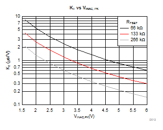
Gate-drive on-time varies proportionately with the error-amplifier output voltage (VCOMP) and inversely proportional to the squared value of the peak of the rectified input voltage sensed through VINAC pin as stated by Equation 3. In Equation 3 it is shown that the on-time is inversely proportionally to the value of resistor RTSET connected between pin TSET and pin AGND. In order to calculate on-time, Equation 4 can be used. Parameter KT is function of the rectified peak input voltage sensed by pin VINAC as reported in graph of Figure 16. In this graph three curves are reported for three different values of RTSET. Two values of parameter KT are reported in Electrical Characteristics the electrical specs table for two values of VINAC: KTL and KTH corresponding at the VINAC = 1.6V and VINAC = 5V and RTSET = 133kΩ. Because voltage on VINAC is proportional to the line rectified voltage, for tON calculation purposes we refer to the peak value of this voltage that is obtained through an internal peak detect. KT is inversely proportional to the squared value of VINAC peak value so it is the tON time realizing the so called voltage feed-forward compensation. The Voltage Feed-forward function modifies the MOSFET on time according to line voltage so, ideally output power delivered does not change if line voltage changes. When operating in single phase mode KT is called KTS and its value is doubled.

The COMP pin voltage value is clamped at 4.95 V, so the maximum on time can be calculated by Equation 4.

Figure 16 shows the values of KT versus the peak voltage value on VINAC pin.
 Figure 16. KT vs Peak Voltage
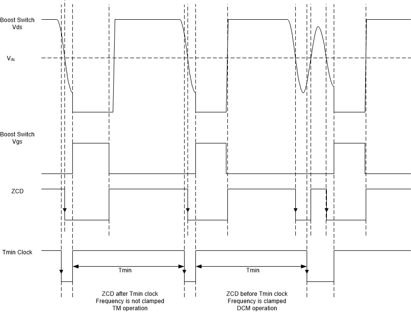
 The maximum switching frequency of each phase is limited by minimum-period timers. If the inductor current decays to zero before the minimum-period timer elapses, the next turn on will be delayed, resulting in discontinuous phase current. As illustrated in Figure 17, when the ZCD signal arrives before the minimum period expires, the ZCD signal is ignored and the controller waits for the next ZCD signal after the minimum period expires to turn on the switch. The minimum switching period, tMIN, is inversely proportional to the time-setting resistor RTSET (the resistor from the TSET pin to ground). The typical tMIN as a function of TSET pin resistor value is shown in Figure 1. The UCC28065 device doubles the clamping frequency compared with UCC28064A. For more detailed comparison between UCC28065 and UCC28064A, refer to the application note "Convert UCC28064A EVM to Higher Switching Frequency Using UCC28065".
 Figure 17. UCC28065 Frequency Clamp
 A restart timer ensures starting under all circumstances by restarting both phases if the ZCD input of either phase has not transitioned from high-to-low within approximately 210 µs.