ZHCSDP7 May 2015 UCC27201A-Q1
PRODUCTION DATA.
8 Application and Implementation
NOTE
Information in the following applications sections is not part of the TI component specification, and TI does not warrant its accuracy or completeness. TI’s customers are responsible for determining suitability of components for their purposes. Customers should validate and test their design implementation to confirm system functionality.
8.1 Application Information
To effect fast switching of power devices and reduce associated switching power losses, a powerful gate driver is employed between the PWM output of controllers and the gates of the power semiconductor devices. Also, gate drivers are indispensable when it is impossible for the PWM controller to directly drive the gates of the switching devices. With the advent of digital power, this situation will be often encountered because the PWM signal from the digital controller is often a 3.3-V logic signal which cannot effectively turn on a power switch. Level shifting circuitry is needed to boost the 3.3-V signal to the gate-drive voltage (such as 12 V) in order to fully turn on the power device and minimize conduction losses. Traditional buffer drive circuits based on NPN/PNP bipolar transistors in totem-pole arrangement, being emitter follower configurations, prove inadequate with digital power because they lack level-shifting capability. Gate drivers effectively combine both the level-shifting and buffer-drive functions. Gate drivers also find other needs such as minimizing the effect of high-frequency switching noise by locating the high-current driver physically close to the power switch, driving gate-drive transformers and controlling floating power-device gates, reducing power dissipation and thermal stress in controllers by moving gate charge power losses from the controller into the driver.
8.2 Typical Application
An open loop half-bridge converter was used to calculate performance in an actual application.
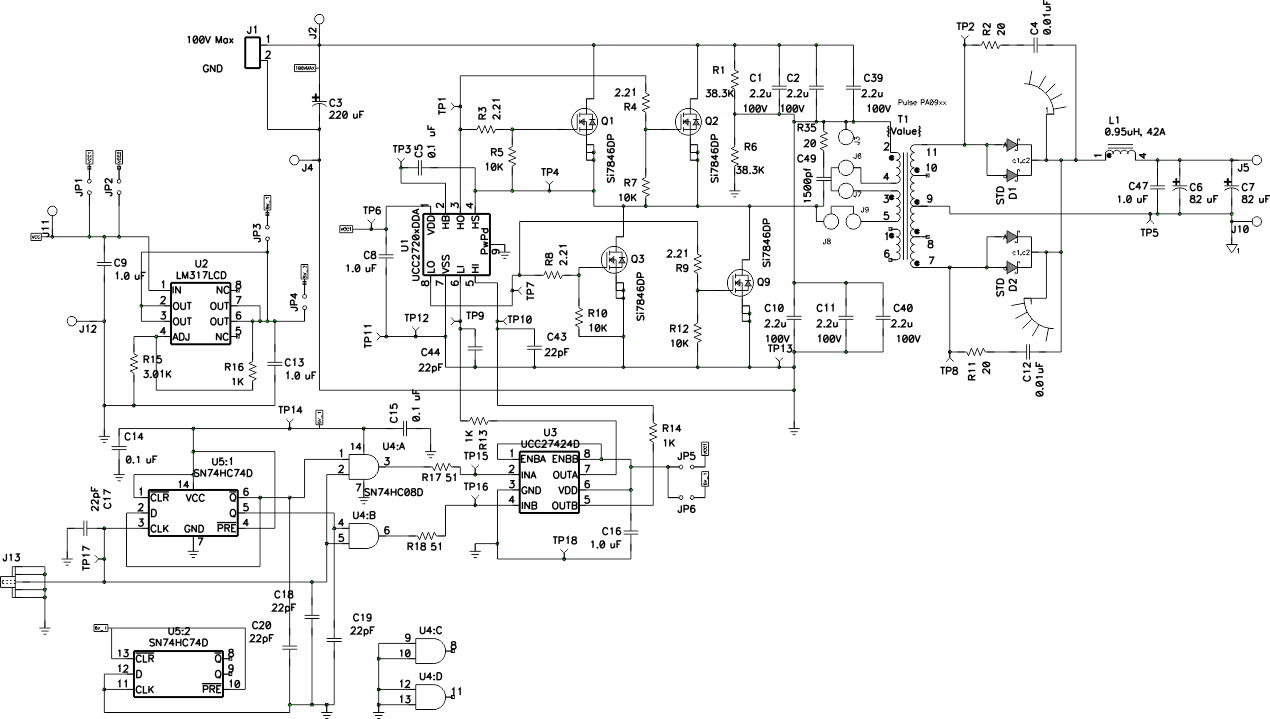 Figure 17. Open Loop Half-Bridge Converter
8.2.1 Design Requirements
Table 2. UCC27201A-Q1 Design Requirements
| DESIGN PARAMETER | EXAMPLE VALUE |
|---|---|
| Supply Voltage, VDD | 12 V |
| Voltage on HS, VHS | 0 V to 100 V |
| Voltage on HB, VHB | 12 V to 112 V |
| Output | 4 V, 20 A |
| Frequency | 200 kHz |
8.2.2 Detailed Design Procedure
8.2.2.1 Switching the MOSFETs
Achieving optimum drive performance at high frequency efficiently requires special attention to layout and minimizing parasitic inductances. Care must be taken at the driver die and package level as well as the PCB layout to reduce parasitic inductances as much as possible. Figure 18 shows the main parasitic inductance elements and current flow paths during the turn ON and OFF of the MOSFET by charging and discharging its CGS capacitance.
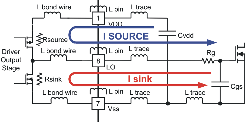 Figure 18. MOSFET Drive Paths and Circuit Parasitics
The ISOURCE current charges the CGS gate capacitor and the ISINK current discharges it. The rise and fall time of the voltage across the gate to source defines how quickly the MOSFET can be switched. Based on actual measurements, the analytical curves in Figure 19 and Figure 20 indicate the output voltage and current of the drivers during the discharge of the load capacitor. Figure 19 shows voltage and current as a function of time. Figure 20 indicates the relationship of voltage and current during fast switching. These figures demonstrate the actual switching process and limitations due to parasitic inductances.
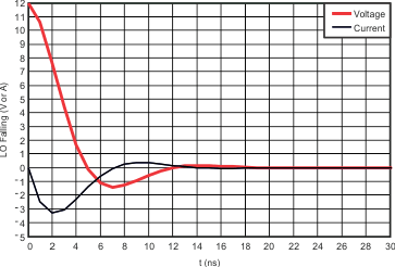
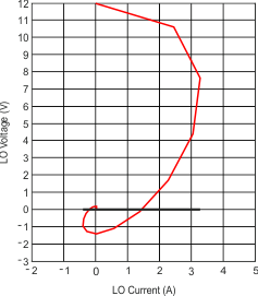 Figure 20. Turn-Off Voltage and Current Switching Diagram
Turning off the MOSFET needs to be achieved as fast as possible to minimize switching losses. For this reason, the UCC27201A-Q1 driver is designed for high peak currents and low output resistance. The sink capability is specified as 0.18 V at 100-mA dc current implying 1.8-Ω RDS(on). With 12-V drive voltage, no parasitic inductance and a linear resistance, one would expect initial sink current amplitude of 6.7 A for both high-side and low-side drivers. Assuming a pure R-C discharge circuit of the gate capacitor, one would expect the voltage and current waveforms to be exponential. Due to the parasitic inductances and non-linear resistance of the driver MOSFET’S, the actual waveforms have some ringing and the peak-sink current of the drivers is approximately 3.3 A as shown in Figure 14. The overall parasitic inductance of the drive circuit is estimated at 4 nH. The internal parasitic inductance of the SOIC-8 package is estimated to be 2 nH including bond wires and leads.
Actual measured waveforms are shown in Figure 21 and Figure 22. As shown, the typical rise time of 8 ns and fall time of 7 ns is conservatively rated.
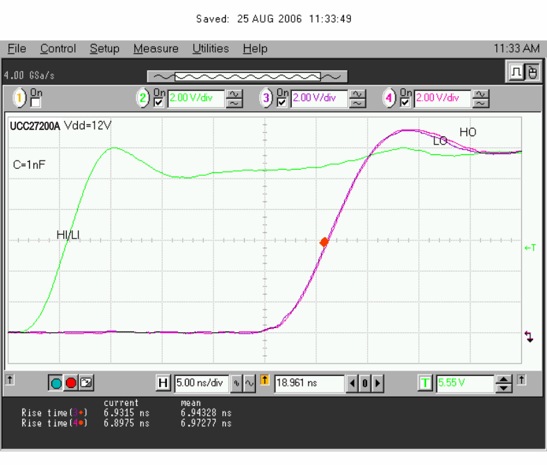 Figure 21. VLO and VHO Rise Time, 1-nF Load, 5 ns/Div
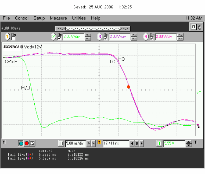 Figure 22. VLO and VHO Fall Time, 1-nF Load, 5-ns/Div
8.2.2.2 Dynamic Switching of the MOSFETs
The true behavior of MOSFETS presents a dynamic capacitive load primarily at the gate to source threshold voltage. Using the turn off case as the example, when the gate to source threshold voltage is reached the drain voltage starts rising, the drain to gate parasitic capacitance couples charge into the gate resulting in the turn off plateau. The relatively low threshold voltages of many MOSFETS and the increased charge that has to be removed (Miller charge) makes good driver performance necessary for efficient switching. An open loop half bridge power converter was utilized to evaluate performance in actual applications. The schematic of the half-bridge converter is shown in Figure 17. The turn off waveforms of the UCC27201A-Q1 driving two MOSFETs in parallel is shown in Figure 23 and Figure 24.
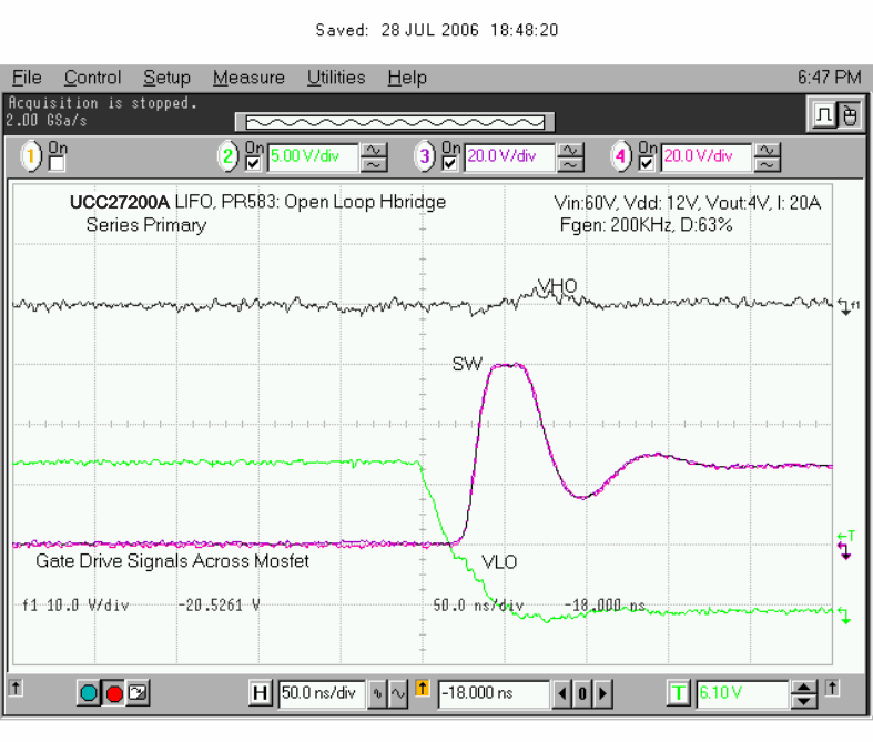 Figure 23. VLO Fall Time in Half-Bridge Converter
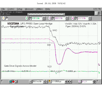 Figure 24. VHO Fall Time in Half-Bridge Converter
8.2.2.3 Delay Matching and Narrow Pulse Widths
The total delays encountered in the PWM, driver and power stage need to be considered for a number of reasons, primarily delay in current limit response. Also to be considered are differences in delays between the drivers which can lead to various concerns depending on the topology. The sync-buck topology switching requires careful selection of dead-time between the high- and low-side switches to avoid 1) cross conduction and 2) excessive body diode conduction. Bridge topologies can be affected by a resulting volt-sec imbalance on the transformer if there is imbalance in the high and low side pulse widths in a steady state condition.
Narrow pulse width performance is an important consideration when transient and short circuit conditions are encountered. Although there may be relatively long steady state PWM output-driver-MOSFET signals, very narrow pulses may be encountered in 1) soft start, 2) large load transients, and 3) short circuit conditions.
The UCC27201A-Q1 driver offers excellent performance regarding high and low-side driver delay matching and narrow pulse width performance. The delay matching waveforms are shown in Figure 25 and Figure 26. The UCC27201A-Q1 driver narrow pulse performance is shown in Figure 27 and Figure 28.
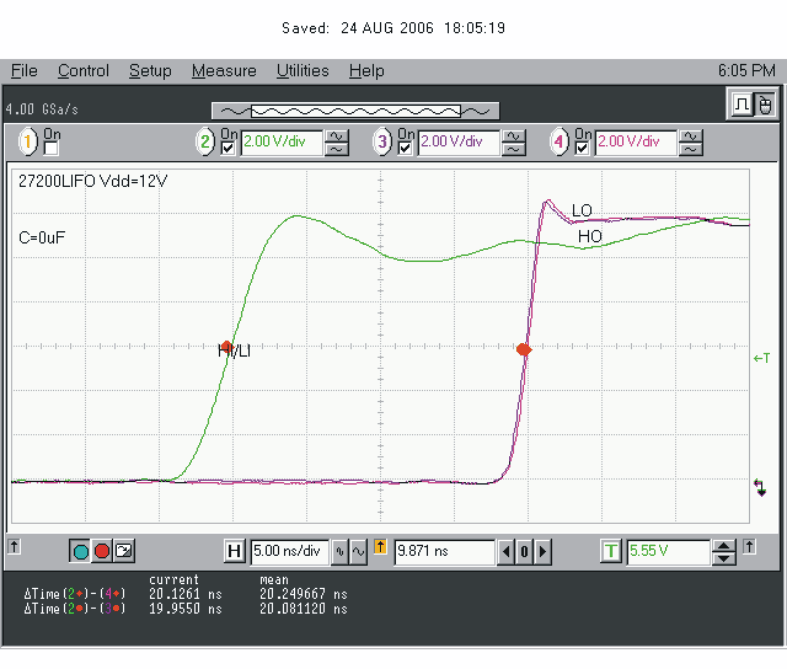 Figure 25. VLO and VHO Rising Edge Delay Matching
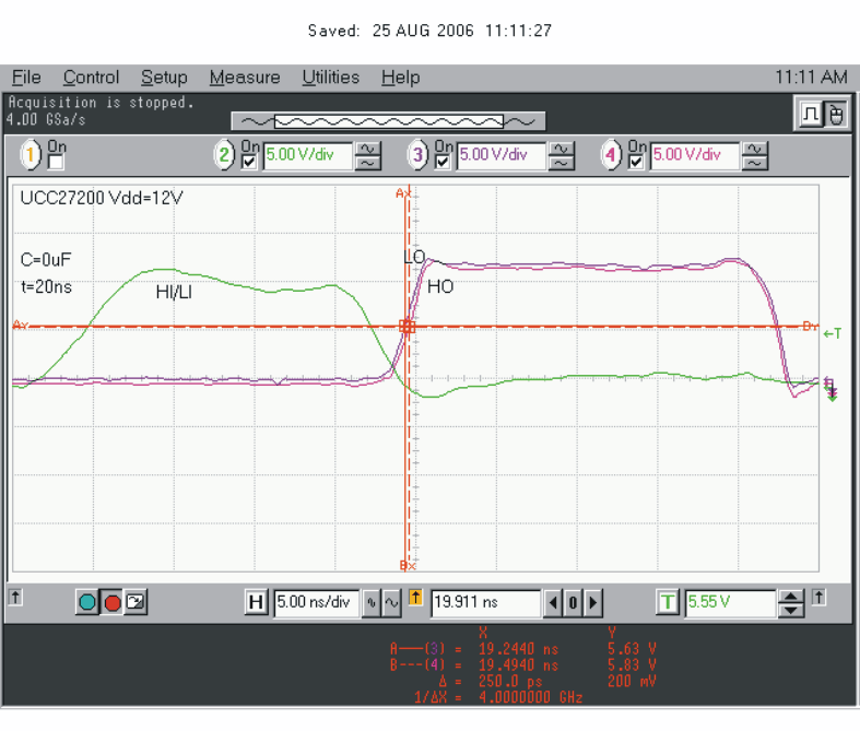 Figure 27. 20-ns Input Pulse Delay Matching
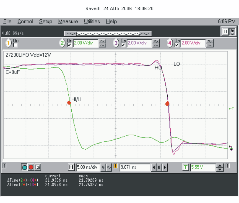 Figure 26. VLO and VHO Falling Edge Delay Matching
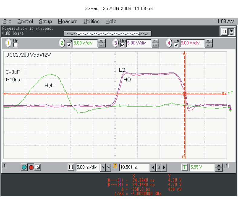 Figure 28. 10-ns Input Pulse Delay Matching
8.2.2.4 Boot Diode Performance
The UCC27201A-Q1 driver incorporates the bootstrap diode necessary to generate the high side bias internally. The characteristics of this diode are important to achieve efficient, reliable operation. The dc characteristics to consider are VF and dynamic resistance. A low VF and high dynamic resistance results in a high forward voltage during charging of the bootstrap capacitor. The UCC27201A-Q1 has a boot diode rated at 0.65-V VF and dynamic resistance of 0.6 Ω for reliable charge transfer to the bootstrap capacitor. The dynamic characteristics to consider are diode recovery time and stored charge. Diode recovery times that are specified with no conditions can be misleading. Diode recovery times at no forward current (IF) can be noticeably less than with forward current applied. The UCC27201A-Q1 boot diode recovery is specified at 20 ns at IF = 20 mA, IREV = 0.5 A. At 0 mA IF, the reverse recovery time is 15 ns.
Another less obvious consideration is how the stored charge of the diode is affected by applied voltage. On every switching transition when the HS node transitions from low to high, charge is removed from the boot capacitor to charge the capacitance of the reverse biased diode. This is a portion of the driver power losses and reduces the voltage on the HB capacitor. At higher applied voltages, the stored charge of the UCC27201A-Q1 PN diode is often less than a comparable Schottky diode.
8.2.3 Application Curves
 Figure 29. VLO Fall Time in Half-Bridge Converter
 Figure 30. VHO Fall Time in Half-Bridge Converter