ZHCSDP7 May 2015 UCC27201A-Q1
PRODUCTION DATA.
5 Pin Configuration and Functions
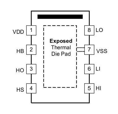
8-Pin SOIC-8 Power Pad
Package DDA
(Top View)

Pin VSS and the exposed thermal die pad are internally connected.
Pin Functions
| PIN | I/O(2) | DESCRIPTION | |
|---|---|---|---|
| NAME | DDA | ||
| HB | 2 | P | High-side bootstrap supply. The bootstrap diode is on-chip but the external bootstrap capacitor is required. Connect positive side of the bootstrap capacitor to this pin. Typical range of HB bypass capacitor is 0.022 μF to 0.1 μF, the value is dependant on the gate charge of the high-side MOSFET however. |
| HI | 5 | I | High-side input. |
| HO | 3 | O | High-side output. Connect to the gate of the high-side power MOSFET. |
| HS | 4 | P | High-side source connection. Connect to source of high-side power MOSFET. Connect negative side of bootstrap capacitor to this pin. |
| LI | 6 | I | Low-side input. |
| LO | 8 | O | Low-side output. Connect to the gate of the low-side power MOSFET. |
| N/C | - | - | No connection. Pins labeled N/C have no connection. |
| PowerPAD™ | Pad(1) | G | Connect to a large thermal mass trace or GND plane to dramatically improve thermal performance. |
| VDD | 1 | P | Positive supply to the lower gate driver. De-couple this pin to VSS (GND). Typical decoupling capacitor range is 0.22 μF to 1.0 μF. |
| VSS | 7 | G | Negative supply terminal for the device which is generally grounded. |
(1) Pin VSS and the exposed thermal die pad are internally connected on the DDA package. Electrically referenced to VSS (GND).
(2) P = Power, G = Ground, I = Input, O = Output, I/O = Input/Output