ZHCSKF2C February 2019 – January 2023 UCC21750
PRODUCTION DATA
- 1 特性
- 2 应用
- 3 说明
- 4 Revision History
- 5 Pin Configuration and Functions
-
6 Specifications
- 6.1 Absolute Maximum Ratings
- 6.2 ESD Ratings
- 6.3 Recommended Operating Conditions
- 6.4 Thermal Information
- 6.5 Power Ratings
- 6.6 Insulation Specifications
- 6.7 Safety Limiting Values
- 6.8 Electrical Characteristics
- 6.9 Safety-Related Certifications
- 6.10 Switching Characteristics
- 6.11 Insulation Characteristics Curves
- 6.12 Typical Characteristics
- 7 Parameter Measurement Information
-
8 Detailed Description
- 8.1 Overview
- 8.2 Functional Block Diagram
- 8.3
Feature Description
- 8.3.1 Power Supply
- 8.3.2 Driver Stage
- 8.3.3 VCC and VDD Undervoltage Lockout (UVLO)
- 8.3.4 Active Pulldown
- 8.3.5 Short Circuit Clamping
- 8.3.6 Internal Active Miller Clamp
- 8.3.7 Desaturation (DESAT) Protection
- 8.3.8 Soft Turn-Off
- 8.3.9 Fault (FLT, Reset, and Enable (RST/EN)
- 8.3.10 Isolated Analog to PWM Signal Function
- 8.4 Device Functional Modes
-
9 Applications and Implementation
- 9.1 Application Information
- 9.2
Typical Application
- 9.2.1 Design Requirements
- 9.2.2
Detailed Design Procedure
- 9.2.2.1 Input Filters for IN+, IN–, and RST/EN
- 9.2.2.2 PWM Interlock of IN+ and IN–
- 9.2.2.3 FLT, RDY, and RST/EN Pin Circuitry
- 9.2.2.4 RST/EN Pin Control
- 9.2.2.5 Turn-On and Turn-Off Gate Resistors
- 9.2.2.6 Overcurrent and Short Circuit Protection
- 9.2.2.7 Isolated Analog Signal Sensing
- 9.2.2.8 Higher Output Current Using an External Current Buffer
- 9.2.3 Application Curves
- 10Power Supply Recommendations
- 11Layout
- 12Device and Documentation Support
- 13Mechanical, Packaging, and Orderable Information
9.2.2.5 Turn-On and Turn-Off Gate Resistors
The UCC21750 features split outputs OUTH and OUTL, which enables the independent control of the turn on and turn off switching speed. The turn on and turn off resistance determine the peak source and sink current, which controls the switching speed in turn. Meanwhile, the power dissipation in the gate driver must be considered to ensure the device is in the thermal limit. At first, the peak source and sink current are calculated as:
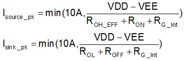
Where
- ROH_EFF is the effective internal pull up resistance of the hybrid pull-up structure, shown in Figure 8-1, which is approximately 2 × ROL, about 0.7 Ω. This is the dominant resistance during the switching transient of the pull up structure.
- ROL is the internal pulldown resistance, about 0.3 Ω.
- RON is the external turn on gate resistance.
- ROFF is the external turn off gate resistance.
- RG_Int is the internal resistance of the SiC MOSFET or IGBT module.
 Figure 9-5 Output Model for Calculating Peak Gate Current
For example, for an IGBT module based system with the following parameters:
- Qg = 3300 nC
- RG_Int = 1.7 Ω
- RON = ROFF = 1 Ω
The peak source and sink current in this case are:
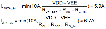
Thus, by using a 1-Ω external gate resistance, the peak source current is 5.9 A, the peak sink current is 6.7 A. The collector-to-emitter dV/dt during the turn on switching transient is dominated by the gate current at the miller plateau voltage. The hybrid pullup structure ensures the peak source current at the miller plateau voltage, unless the turn on gate resistor is too high. The faster the collector-to-emitter, Vce, voltage rises to VDC, the smaller the turn on switching loss is. The dV/dt can be estimated as Qgc/Isource_pk. For the turn off switching transient, the drain-to-source dV/dt is dominated by the load current, unless the turn off gate resistor is too high. After Vce reaches the dc bus voltage, the power semiconductor is in saturation mode and the channel current is controlled by Vge. The peak sink current determines the dI/dt, which dominates the Vce voltage overshoot accordingly. If using relatively large turn off gate resistance, the Vce overshoot can be limited. The overshoot can be estimated by:

Where
- Lstray is the stray inductance in power switching loop, as shown in Figure 9-6
- Iload is the load current, which is the turn off current of the power semiconductor
- Cies is the input capacitance of the power semiconductor
- Vplat is the plateau voltage of the power semiconductor
- Vth is the threshold voltage of the power semiconductor
 Figure 9-6 Stray Parasitic Inductance of IGBTs in a Half-Bridge Configuration
The power dissipation must be taken into account to maintain the gate driver within the thermal limit. The power loss of the gate driver includes the quiescent loss and the switching loss, which can be calculated as:

PQ is the quiescent power loss for the driver, which is Iq x (VDD-VEE) = 5 mA × 20 V = 0.100 W. The quiescent power loss is the power consumed by the internal circuits such as the input stage, reference voltage, logic circuits, protection circuits when the driver is switching when the driver is biased with VDD and VEE, and also the charging and discharing current of the internal circuit when the driver is switching. The power dissipation when the driver is switching can be calculated as:

Where
- Qg is the gate charge required at the operation point to fully charge the gate voltage from VEE to VDD
- fsw is the switching frequency
In this example, the PSW can be calculated as:

Thus, the total power loss is:

When the board temperature is 125°C, the junction temperature can be estimated as:
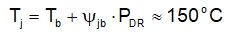
Therefore, for the application in this example, with 125°C board temperature, the maximum switching frequency is approximately 50 kHz to keep the gate driver in the thermal limit. By using a lower switching frequency, or increasing external gate resistance, the gate driver can be operated at a higher switching frequency.