ZHCSRT9E january 2007 – march 2023 TXB0101
PRODUCTION DATA
- 1 特性
- 2 应用
- 3 说明
- 4 Revision History
- 5 Pin Configuration and Functions
-
6 Specification
- 6.1 Absolute Maximum Ratings
- 6.2 ESD Ratings
- 6.3 Recommended Operating Conditions
- 6.4 Thermal Information
- 6.5 Electrical Characteristics
- 6.6 Timing Requirements, VCCA = 1.2 V
- 6.7 Timing Requirements, VCCA = 1.5 V ± 0.1 V
- 6.8 Timing Requirements, VCCA = 1.8 V ± 0.15 V
- 6.9 Timing Requirements, VCCA = 2.5 V ± 0.2 V
- 6.10 Timing Requirements, VCCA = 3.3 V ± 0.3 V
- 6.11 Switching Characteristics, VCCA = 1.2 V
- 6.12 Switching Characteristics, VCCA = 1.5 V ± 0.1 V
- 6.13 Switching Characteristics, VCCA = 1.8 V ± 0.15 V
- 6.14 Switching Characteristics, VCCA = 2.5 V ± 0.2 V
- 6.15 Switching Characteristics, VCCA = 3.3 V ± 0.3 V
- 6.16 Operating Characteristics
- 6.17 Typical Characteristics
- 7 Detailed Description
- 8 Application and Implementation
- 9 Device and Documentation Support
- 10Mechanical, Packaging, and Orderable Information
封装选项
机械数据 (封装 | 引脚)
散热焊盘机械数据 (封装 | 引脚)
- DCK|6
订购信息
7.3.1 Architecture
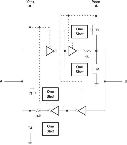
The TXB0101 architecture (see Figure 7-1) does not require a direction-control signal to control the direction of data flow from A to B or from B to A. In a DC state, the output drivers of the TXB0101 can maintain a high or low, but are designed to be weak, so that they can be overdriven by an external driver when data on the bus starts flowing the opposite direction.
The output one-shots detect rising or falling edges on the A or B ports. During a rising edge, the one-shot turns on the PMOS transistors (T1, T3) for a short duration, which speeds up the low-to-high transition. Similarly, during a falling edge, the one-shot turns on the NMOS transistors (T2, T4) for a short duration, which speeds up the high-to-low transition. The typical output impedance during output transition is 70 Ω at VCCO = 1.2 V to 1.8 V, 50 Ω at VCCO = 1.8 V to 3.3 V, and 40 Ω at VCCO = 3.3 V to 5 V.
 Figure 7-1 Architecture of TXB0101 I/O Cell