ZHCSD29A November 2014 – November 2014 TVB1440
PRODUCTION DATA.
- 1 特性
- 2 应用
- 3 说明
- 4 简化电路原理图
- 5 修订历史记录
- 6 Pin Configuration and Functions
- 7 Specifications
- 8 Detailed Description
- 9 Application and Implementation
- 10Power Supply Recommendations
- 11Layout
- 12器件和文档支持
- 13机械封装和可订购信息
6 Pin Configuration and Functions
VQFN 0.5 mm Pitch
RGZ 48 Pin
Top View
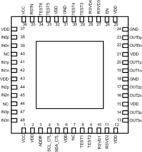
Pin Functions
| PIN | DESCRIPTION | ||
|---|---|---|---|
| SIGNAL | NO. | I/O | |
| DATA LANES PINS | |||
| IN0p, IN0n | 38, 39 | Input (100Ω diff) |
Lane 0 Differential Input |
| IN1p, IN1n | 41, 42 | Lane 1 Differential Input | |
| IN2p, IN2n | 44, 45 | Lane 2 Differential Input | |
| IN3p, IN3n | 47, 48 | Lane 3 Differential Input | |
| OUT0p, OUT0n | 23, 22 | Output (100Ω diff) |
Lane 0 Differential Output |
| OUT1p, OUT1n | 20, 19 | Lane 1 Differential Output | |
| OUT2p, OUT2n | 17, 16 | Lane 2 Differential Output | |
| OUT3p, OUT3n | 14, 13 | Lane 3 Differential Output | |
| CONTROL PINS | |||
| ADDR | 3 | 3-level Input | I2C Target Address Select. |
| EN | 26 | I | Device Enable. This input incorporates internal pullup of 200 kΩ. |
| NC | 7, 40, 46 | No Connect. These terminals may be left un-connected, or connect to GND. | |
| RSTN | 35 | I | Active Low Device Reset. This is 1.1V input. This input includes a 150kΩ resistor to the VDDD core supply. An external capacitor to GND is recommended on the RSTN input to provide a power-up delay. This signal is used to place the TVB1440 into Shutdown mode for the lowest power consumption. When the RSTN input is asserted, all outputs are high-impedance, and inputs are ignored; all I2C registers are reset to their default values. At power up, the RSTN input must not be de-asserted until the VCC and VDD supplies have reached at least the minimum recommended supply voltage level. |
| RSVD1 | 10 | I | Reserved pins. Please connect the pin to GND through 1K resistor. |
| RSVD2 | 11 | I | Reserved pins. Please connect the pin to VCC through 1K resistor. |
| RSVD3 | 27 | I | Reserved pins. Please connect the pin to VCC through 1K resistor. |
| RSVD4 | 28 | I | Reserved pins. Please connect the pin to GND through 1K resistor. |
| SCL_CTL SDA_CTL |
4 5 |
I/O | Bidirectional I2C interface to configure TVB1440. This interface is active independent of EN input but inactive when RSTN is low. |
| TEST1-6 | 8, 9, 29, 30, 33, 34 | Test Outputs. Do not connect. | |
| SUPPLY AND GROUND PINS | |||
| GND | 18, 24, 31, PAD | Ground. Reference GND connections include the device package exposed thermal pad. | |
| VDD | 2, 6, 12, 15, 21, 25, 32, 37, 43 | Low voltage supply for analog and digital core. Nominally 1.1V | |
| VCC | 1, 36 | 3.3V Supply | |