ZHCSD29A November 2014 – November 2014 TVB1440
PRODUCTION DATA.
- 1 特性
- 2 应用
- 3 说明
- 4 简化电路原理图
- 5 修订历史记录
- 6 Pin Configuration and Functions
- 7 Specifications
- 8 Detailed Description
- 9 Application and Implementation
- 10Power Supply Recommendations
- 11Layout
- 12器件和文档支持
- 13机械封装和可订购信息
11 Layout
11.1 Layout Guidelines
11.1.1 Differential Pairs
This section describes the layout recommendations for all the TVB1440 differential pairs: IN[3:0] and OUT[3:0].
- Must be designed with a differential impedance of 100 Ω ± 10% or 50-Ω single-ended impedance.
- In order to minimize cross talk, it is recommended to keep high speed signals away from each other. Each pair should be separated by at least 5 times the signal trace width.
- Route all differential pairs on the same layer adjacent to a solid ground plane.
- Do not route differential pairs over any plane split.
- Adding test points causes impedance discontinuity and; therefore, negative impacts signal performance. If test points are used, they should be placed in series and symmetrically. They must not be placed in a manner that causes stub on the differential pair.
- Avoid 90 degree turns in trace. The use of bends in differential traces should be kept to a minimum. When bends are used, the number of left and right bends should be as equal as possible and the angle of the bend should be ≥ 135 degrees. This minimizes any length mismatch causes by the bends; and therefore, minimizes the impact bends have on EMI.
- Minimize the trace lengths of the differential pair traces. Longer trace lengths require very careful routing to assure proper signal integrity.
- Keep intra-pair skew to a minimum in order to minimize EMI. There should be less than 5 mils difference between a differential pair signal and its complement.
- Minimize the use of vias in the differential pair paths as much as possible. If this is not practical, make sure that the same via type and placement are used for both signals in a pair. It is recommended to keep the vias count to 2 or less.
11.1.2 Layout Example
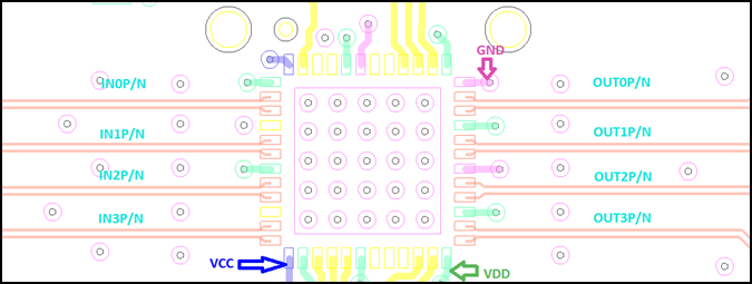 Figure 16. TBV1440 Layout
11.1.3 Placement
- A 100-nF should be placed as close as possible on each VDD and VCC power pin.
- The 100-nF capacitors on the IN[3:0] and OUT[3:0] nets should be placed close to the connector.
- The ESD and EMI protection devices (if used) should also be placed as possible to the connector.
11.1.4 Package Specific
- The TVB1440 package as a 0.5 mm pin pitch
- The TVB1440 package has a 4.1 mm x 4.1 mm thermal pad. This thermal pad must be connected to ground through a system of vias.
- All vias under device, except for those connected to thermal pad, should be solder masked to avoid any potential issues with thermal pad layouts.
11.1.5 Ground
It is recommended that only one board plane be used in the design. This provides the best image plane for signal traces running above the plane. The thermal pad of the TVB1440 should be connected to this plane through a system of vias.