ZHCSD29A November   2014  – November 2014 TVB1440

PRODUCTION DATA.  

  1. 特性
  2. 应用
  3. 说明
  4. 简化电路原理图
  5. 修订历史记录
  6. Pin Configuration and Functions
  7. Specifications
    1. 7.1 Absolute Maximum Ratings
    2. 7.2 Handling Ratings
    3. 7.3 Recommended Operating Conditions
    4. 7.4 Thermal Information
    5. 7.5 Electrical Characteristics
    6. 7.6 Timing Requirements
    7. 7.7 Switching Characteristics
    8. 7.8 Typical Characteristics
  8. Detailed Description
    1. 8.1 Overview
    2. 8.2 Functional Block Diagram
    3. 8.3 Feature Description
      1. 8.3.1 Equalization
      2. 8.3.2 Configurable Output
      3. 8.3.3 Squelch
    4. 8.4 Device Functional Modes
      1. 8.4.1 Active Mode
      2. 8.4.2 Shutdown Mode
      3. 8.4.3 Squelch Mode
    5. 8.5 Programming
      1. 8.5.1 Local I2C Interface
      2. 8.5.2 Receiver (IN[3:0]P/N) Adjustments
        1. 8.5.2.1 Equalization Level
        2. 8.5.2.2 Squelch Level
      3. 8.5.3 Main Link Output [OUT[3:0]P/N] Adjustments
        1. 8.5.3.1 LINK Address Space
      4. 8.5.4 Example Script
    6. 8.6 Register Maps
  9. Application and Implementation
    1. 9.1 Application Information
      1. 9.1.1 Typical Application
        1. 9.1.1.1 Design Requirements
        2. 9.1.1.2 Detailed Design Procedure
          1. 9.1.1.2.1 Common 4k2k TV Panel Configuration
          2. 9.1.1.2.2 1Max Stream Rate
          3. 9.1.1.2.3 Encoded Stream Rate
          4. 9.1.1.2.4 TVB1440 Configuration
          5. 9.1.1.2.5 Receiver Equalization Setting
          6. 9.1.1.2.6 Transmitter Settings
          7. 9.1.1.2.7 RESET
  10. 10Power Supply Recommendations
    1. 10.1 Power-Up Sequence
    2. 10.2 Power-Down Sequence
  11. 11Layout
    1. 11.1 Layout Guidelines
      1. 11.1.1 Differential Pairs
      2. 11.1.2 Layout Example
      3. 11.1.3 Placement
      4. 11.1.4 Package Specific
      5. 11.1.5 Ground
  12. 12器件和文档支持
    1. 12.1 商标
    2. 12.2 静电放电警告
    3. 12.3 Export Control Notice
    4. 12.4 术语表
  13. 13机械封装和可订购信息

封装选项

机械数据 (封装 | 引脚)
散热焊盘机械数据 (封装 | 引脚)
订购信息

10 Power Supply Recommendations

The following power-up and power-down sequences describe how the RSTN signal is applied to the TVB1440.

10.1 Power-Up Sequence

  1. Apply VDD then VCC (recommended both less than 10-ms ramp time). VDD must be asserted first and stable for greater than 10 μs before VCC is applied.
  2. RSTN must remain asserted until VCC/VDD voltage has reached minimum recommended operation for more than 100 μs.
  3. De-assert RSTN (Note: This RSTN is a 1.1V interface and is internally connected to VDD through a 150-kΩ resistor).
  4. Device will be available for operation approximately 400 ms after a valid reset.
power_up_sequence_slase51.gif
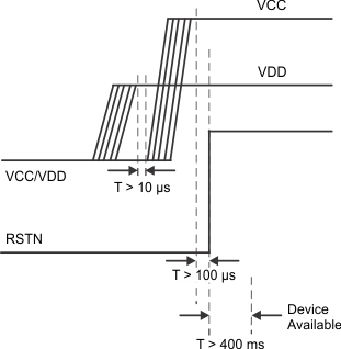
Figure 15. Power-up Sequence

10.2 Power-Down Sequence

There is no power-down sequence required.