ZHCSAJ8C November 2012 – October 2016 TS5A3159-Q1
PRODUCTION DATA.
- 1 特性
- 2 应用范围
- 3 说明
- 4 修订历史记录
- 5 Pin Configuration and Functions
-
6 Specifications
- 6.1 Absolute Maximum Ratings
- 6.2 ESD Ratings
- 6.3 Recommended Operating Conditions
- 6.4 Thermal Information
- 6.5 Electrical Characteristics for 5-V Supply
- 6.6 Electrical Characteristics for 3.3-V Supply
- 6.7 Electrical Characteristics For 2.5-V Supply
- 6.8 Electrical Characteristics For 1.8-V Supply
- 6.9 Typical Characteristics
- 7 Parameter Measurement Information
- 8 Detailed Description
- 9 Applications and Implementation
- 10Power Supply Recommendations
- 11Layout
- 12器件和文档支持
- 13机械、封装和可订购信息
11 Layout
11.1 Layout Guidelines
TI recommends to keep signal lines as short as possible. Incorporation of microstrip or stripline techniques is also recommended when signal lines are greater than 1 inch in length. These traces must be designed with a characteristic impedance of either 50 Ω or 75 Ω, as required by the application. Do not place this device too close to high voltage switching components, as they may cause interference.
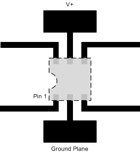
11.2 Layout Example
 Figure 22. Layout Example