ZHCSAJ8C November 2012 – October 2016 TS5A3159-Q1
PRODUCTION DATA.
- 1 特性
- 2 应用范围
- 3 说明
- 4 修订历史记录
- 5 Pin Configuration and Functions
-
6 Specifications
- 6.1 Absolute Maximum Ratings
- 6.2 ESD Ratings
- 6.3 Recommended Operating Conditions
- 6.4 Thermal Information
- 6.5 Electrical Characteristics for 5-V Supply
- 6.6 Electrical Characteristics for 3.3-V Supply
- 6.7 Electrical Characteristics For 2.5-V Supply
- 6.8 Electrical Characteristics For 1.8-V Supply
- 6.9 Typical Characteristics
- 7 Parameter Measurement Information
- 8 Detailed Description
- 9 Applications and Implementation
- 10Power Supply Recommendations
- 11Layout
- 12器件和文档支持
- 13机械、封装和可订购信息
9 Applications and Implementation
NOTE
Information in the following applications sections is not part of the TI component specification, and TI does not warrant its accuracy or completeness. TI’s customers are responsible for determining suitability of components for their purposes. Customers should validate and test their design implementation to confirm system functionality.
9.1 Application Information
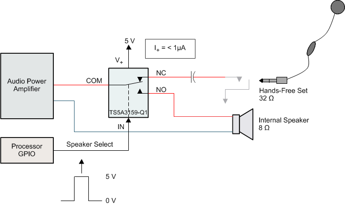
Analog switches are commonly used in battery powered applications to route audio signals. A typical use case is highlighted in Figure 20. The analog switch is supplied with 5 V and the control input is from a 5-V processor GPIO. In this case, there are no concerns related to excess power consumption.
9.2 Typical Application
 Figure 20. Typical Application Schematic
9.2.1 Design Requirements
In this application example, the device receives the control signal from a 5-V GPIO and common input from an Audio Power amplifier. The input is routed to either the Hands free set or the internal speaker depending upon the control signal.
9.2.2 Detailed Design Procedure
Since the control signal varies from 0 to 5 V (Vdd), there’s no excess current consumption. However, if the control signal comes from lower voltage GPIOs while the V+ of TS5A3159 is connected to the battery whose voltage varies, it can lead to an excess current draw from the V+ suppl pin. Such a scenario requires the use of an external voltage level translator such as the SN74LVC1T45. For more information see Preventing Excess Current Consumption on Analog Switches, SCDA011.
9.2.3 Application Curve
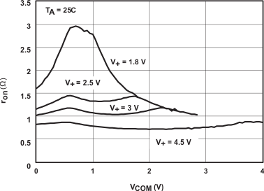
The ON state resistance of the switch is a critical parameter to measure since it helps select the right switch for the application. The on state resistance versus the common voltage can be seen in Figure 21.
