ZHCSMP8B November 2020 – March 2021 TPSM5D1806
PRODUCTION DATA
- 1 特性
- 2 应用
- 3 说明
- 4 Revision History
- 5 Pin Configuration and Functions
- 6 Specifications
-
7 Detailed Description
- 7.1 Overview
- 7.2 Functional Block Diagram
- 7.3
Feature Description
- 7.3.1 Adjustable Output Voltage
- 7.3.2 Frequency Selection
- 7.3.3 Minimum and Maximum Input Voltage
- 7.3.4 Recommended Settings
- 7.3.5 Device Mode Configuration
- 7.3.6 Input Capacitors
- 7.3.7 Minimum Required Output Capacitance
- 7.3.8 Ambient Temperature Versus Total Power Dissipation
- 7.3.9 Remote Sense
- 7.3.10 Enable (EN) and Under Voltage Lockout (UVLO)
- 7.3.11 Soft Start
- 7.3.12 Power Good
- 7.3.13 Safe Start-up into Pre-Biased Outputs
- 7.3.14 BP5
- 7.3.15 Overcurrent Protection
- 7.3.16 Thermal Shutdown
- 7.4 Device Functional Modes
- 8 Application and Implementation
- 9 Power Supply Recommendations
- 10Layout
- 11Device and Documentation Support
- 12Mechanical, Packaging, and Orderable Information
7.3.1 Adjustable Output Voltage
When operating the TPSM5D1806 as a dual output device, the two output voltages (VOUT1 and VOUT2) are set using resistor dividers between the output voltages and AGND with the mid-point of the resistor divider connecting to the corresponding feedback pin (FB1 and FB2). See Figure 7-4.
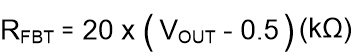
Select a bottom feedback resistor of 10 kΩ and calculate the value for the top feedback resistor (RFBT) using the following equation. It is recommended to use divider resistors with 1% tolerance or better, and with temperature coefficient of 100 ppm or lower.
When connecting the two outputs of the TPSM5D1806 for current sharing, the output voltage is set using only a single feedback divider connected to FB1. The FB pin of the second channel, FB2, must be left floating as shown in Figure 7-2. Use Equation 1 to calculate the RFBT.
 Figure 7-1 Single Device, Dual
Output
Figure 7-1 Single Device, Dual
Output Figure 7-2 Single Device, Current
Sharing
Figure 7-2 Single Device, Current
Sharing