ZHCSMP8B November   2020  – March 2021 TPSM5D1806

PRODUCTION DATA  

  1. 特性
  2. 应用
  3. 说明
  4. Revision History
  5. Pin Configuration and Functions
  6. Specifications
    1. 6.1 Absolute Maximum Ratings
    2. 6.2 ESD Ratings
    3. 6.3 Recommended Operating Conditions
    4. 6.4 Thermal Information
    5. 6.5 Electrical Characteristics
    6. 6.6 Typical Characteristics (VIN = 12 V)
    7. 6.7 Typical Characteristics (VIN = 5 V)
  7. Detailed Description
    1. 7.1 Overview
    2. 7.2 Functional Block Diagram
    3. 7.3 Feature Description
      1. 7.3.1  Adjustable Output Voltage
      2. 7.3.2  Frequency Selection
        1. 7.3.2.1 Synchronization
        2. 7.3.2.2 Allowable Switching Frequency
      3. 7.3.3  Minimum and Maximum Input Voltage
      4. 7.3.4  Recommended Settings
      5. 7.3.5  Device Mode Configuration
        1. 7.3.5.1 MODE1 (Operating Mode and Phase Position)
        2. 7.3.5.2 MODE2 (Setting the Switching Frequency)
      6. 7.3.6  Input Capacitors
      7. 7.3.7  Minimum Required Output Capacitance
      8. 7.3.8  Ambient Temperature Versus Total Power Dissipation
      9. 7.3.9  Remote Sense
      10. 7.3.10 Enable (EN) and Under Voltage Lockout (UVLO)
      11. 7.3.11 Soft Start
      12. 7.3.12 Power Good
      13. 7.3.13 Safe Start-up into Pre-Biased Outputs
      14. 7.3.14 BP5
      15. 7.3.15 Overcurrent Protection
      16. 7.3.16 Thermal Shutdown
    4. 7.4 Device Functional Modes
      1. 7.4.1 Active Mode
      2. 7.4.2 Shutdown Mode
  8. Application and Implementation
    1. 8.1 Application Information
    2. 8.2 Typical Application (Dual Outputs)
      1. 8.2.1 Design Requirements
      2. 8.2.2 Detailed Design Procedure
        1. 8.2.2.1 Custom Design With WEBENCH® Tools
        2. 8.2.2.2 Output Voltage Setpoint
        3. 8.2.2.3 Input Capacitors
        4. 8.2.2.4 Output Capacitor Selection
      3. 8.2.3 Typical Application (Paralleled Outputs)
        1. 8.2.3.1 Design Requirements
        2. 8.2.3.2 Detailed Design Procedure
          1. 8.2.3.2.1 Output Voltage Setpoint
          2. 8.2.3.2.2 Input Capacitors
          3. 8.2.3.2.3 Output Capacitor Selection
  9. Power Supply Recommendations
  10. 10Layout
    1. 10.1 Layout Guidelines
    2. 10.2 Layout Examples
      1. 10.2.1 Package Specifications
      2. 10.2.2 EMI
  11. 11Device and Documentation Support
    1. 11.1 Device Support
      1. 11.1.1 Development Support
        1. 11.1.1.1 Custom Design With WEBENCH® Tools
    2. 11.2 接收文档更新通知
    3. 11.3 支持资源
    4. 11.4 Trademarks
    5. 11.5 静电放电警告
    6. 11.6 术语表
  12. 12Mechanical, Packaging, and Orderable Information

封装选项

机械数据 (封装 | 引脚)
散热焊盘机械数据 (封装 | 引脚)
订购信息
Output Voltage Setpoint

The output voltage of the TPSM5D1806 device is externally adjustable using a resistor divider. The recommended value of RFBB is 10 kΩ. The value for RFBT can be calculated using Equation 5:

Equation 5. GUID-ED4F3335-EDD9-43BE-A158-E480D4DFCB2A-low.gif

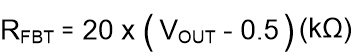
For the desired output voltage of 0.9 V, the formula yields a value of 8 kΩ. Choose the closest available value of 8.06 kΩ for RFBT or place two resistors in series to come closer to the exact value.