ZHCSKO1B December 2019 – September 2021 TPSM53603
PRODUCTION DATA
- 1 特性
- 2 应用
- 3 说明
- 4 Revision History
- 5 Pin Configuration and Functions
- 6 Specifications
-
7 Detailed Description
- 7.1 Overview
- 7.2 Functional Block Diagram
- 7.3
Feature Description
- 7.3.1 Adjusting the Output Voltage
- 7.3.2 Switching Frequency
- 7.3.3 Input Capacitors
- 7.3.4 Output Capacitors
- 7.3.5 Output On/Off Enable (EN)
- 7.3.6 Programmable Undervoltage Lockout (UVLO)
- 7.3.7 Power Good (PGOOD)
- 7.3.8 Light Load Operation
- 7.3.9 Voltage Dropout
- 7.3.10 Overcurrent Protection (OCP)
- 7.3.11 Thermal Shutdown
- 7.4 Device Functional Modes
- 8 Application and Implementation
- 9 Power Supply Recommendations
- 10Layout
- 11Device and Documentation Support
- 12Mechanical, Packaging, and Orderable Information
7.3.1 Adjusting the Output Voltage
A resistor divider connected to the FB pin (pin 9) sets the output voltage of the TPSM53603. The output voltage adjustment range is from 1 V to 7 V. Figure 7-1 shows the feedback resistor connections for setting the output voltage. The recommended value of RFBT is 10 kΩ. The value for RFBB can be calculated using Equation 1. Table 7-1 lists the standard resistor values for several output voltages. The minimum required output capacitance for each output voltage is also included in Table 7-1. The capacitance values listed represent the effective capacitance, taking into account the effects of DC bias and temperature variation.
Equation 1. 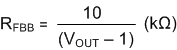
 Figure 7-1 Setting the Output Voltage
Table 7-1 Setting the Output Voltage
| VOUT (V) | RFBB (kΩ)(1) | COUT(MIN) (µF) (EFFECTIVE) | VOUT (V) | RFBB (kΩ)(1) | COUT(MIN) (µF) (EFFECTIVE) | |
|---|---|---|---|---|---|---|
| 1.0 | open | 150 | 3.0 | 4.99 | 48 | |
| 1.1 | 100 | 140 | 3.3 | 4.32 | 43 | |
| 1.2 | 49.9 | 128 | 4.0 | 3.32 | 35 | |
| 1.3 | 33.2 | 117 | 4.5 | 2.87 | 31 | |
| 1.4 | 24.9 | 108 | 5.0 | 2.49 | 28 | |
| 1.5 | 20.0 | 101 | 5.5 | 2.21 | 25 | |
| 1.8 | 12.4 | 83 | 6.0 | 2.00 | 23 | |
| 2.0 | 10.0 | 74 | 6.5 | 1.82 | 21 | |
| 2.5 | 6.65 | 58 | 7.0 | 1.65 | 19 |
(1) RFBT = 10.0 kΩ