ZHCSKO1B December 2019 – September 2021 TPSM53603
PRODUCTION DATA
- 1 特性
- 2 应用
- 3 说明
- 4 Revision History
- 5 Pin Configuration and Functions
- 6 Specifications
-
7 Detailed Description
- 7.1 Overview
- 7.2 Functional Block Diagram
- 7.3
Feature Description
- 7.3.1 Adjusting the Output Voltage
- 7.3.2 Switching Frequency
- 7.3.3 Input Capacitors
- 7.3.4 Output Capacitors
- 7.3.5 Output On/Off Enable (EN)
- 7.3.6 Programmable Undervoltage Lockout (UVLO)
- 7.3.7 Power Good (PGOOD)
- 7.3.8 Light Load Operation
- 7.3.9 Voltage Dropout
- 7.3.10 Overcurrent Protection (OCP)
- 7.3.11 Thermal Shutdown
- 7.4 Device Functional Modes
- 8 Application and Implementation
- 9 Power Supply Recommendations
- 10Layout
- 11Device and Documentation Support
- 12Mechanical, Packaging, and Orderable Information
10.3 Theta JA versus PCB Area
The amount of PCB copper affects the thermal performance of the device. Figure 10-4 shows the effects of copper area on the junction-to-ambient thermal resistance (RθJA) of the TPSM53603. The junction-to-ambient thermal resistance is plotted for a 4-layer PCB with PCB area from 30 cm2 to 80 cm2.
To determine the required copper area for an application:
- Determine the maximum power dissipation of the device in the application by referencing the power dissipation graphs in Section 6.6 through Section 6.9.
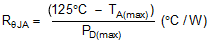
- Calculate the maximum RθJA using Equation 3 and the maximum ambient temperature of the application.
Equation 3.
- Reference Figure 10-4 to determine the minimum required PCB area for the application conditions.
") Figure 10-4 RθJA versus PCB Area (per Layer)
Figure 10-4 RθJA versus PCB Area (per Layer)