ZHCSLS0B July 2022 – April 2024 TPS929240-Q1
PRODUCTION DATA
- 1
- 1 特性
- 2 应用
- 3 说明
- 4 Pin Configuration and Functions
- 5 Specifications
-
6 Detailed Description
- 6.1 Overview
- 6.2 Functional Block Diagram
- 6.3
Feature Description
- 6.3.1 Device Bias and Power
- 6.3.2 Constant Current Output
- 6.3.3 PWM Dimming
- 6.3.4 FAIL-SAFE State Operation
- 6.3.5 On-Chip, 8-Bit, Analog-to-Digital Converter (ADC)
- 6.3.6
Diagnostic and Protection in NORMAL State
- 6.3.6.1 VBAT Undervoltage Lockout Diagnostics in NORMAL state
- 6.3.6.2 Low-Supply Warning Diagnostics in NORMAL State
- 6.3.6.3 Supply Undervoltage Diagnostics in NORMAL State
- 6.3.6.4 Reference Diagnostics in NORMAL state
- 6.3.6.5 Pre-Thermal Warning in NORMAL state
- 6.3.6.6 Overtemperature Protection in NORMAL state
- 6.3.6.7 Overtemperature Shutdown in NORMAL state
- 6.3.6.8 LED Open-Circuit Diagnostics in NORMAL state
- 6.3.6.9 LED Short-Circuit Diagnostics in NORMAL state
- 6.3.6.10 Single-LED Short-Circuit Detection in NORMAL state
- 6.3.6.11 EEPROM CRC Error in NORMAL state
- 6.3.6.12 Communication Loss Diagnostic in NORMAL State
- 6.3.6.13 Fault Masking in NORMAL state
- 53
- 6.3.7
Diagnostic and Protection in FAIL-SAFE states
- 6.3.7.1 Supply Undervoltage Lockout Diagnostics in FAIL-SAFE states
- 6.3.7.2 Low-Supply Warning Diagnostics in FAIL-SAFE states
- 6.3.7.3 Supply Undervoltage Diagnostics in FAIL-SAFE State
- 6.3.7.4 Reference Diagnostics in FAIL-SAFE states
- 6.3.7.5 Pre-Thermal Warning in FAIL-SAFE state
- 6.3.7.6 Overtemperature Protection in FAIL-SAFE state
- 6.3.7.7 Overtemperature Shutdown in FAIL-SAFE state
- 6.3.7.8 LED Open-Circuit Diagnostics in FAIL-SAFE state
- 6.3.7.9 LED Short-Circuit Diagnostics in FAIL-SAFE state
- 6.3.7.10 Single-LED Short-Circuit Detection in FAIL-SAFE state
- 6.3.7.11 EEPROM CRC Error in FAIL-SAFE State
- 6.3.7.12 Fault Masking in FAIL-SAFE state
- Diagnostics Table in FAIL-SAFE State
- 6.3.8 OFAF Setup In FAIL-SAFE state
- 6.3.9 ERR Output
- 6.4 Device Functional Modes
- 6.5 Programming
- 6.6 Register Maps
- 7 Application and Implementation
- 8 Device and Documentation Support
- 9 Revision History
- 10Mechanical, Packaging, and Orderable Information
封装选项
请参考 PDF 数据表获取器件具体的封装图。
机械数据 (封装 | 引脚)
- DCP|38
散热焊盘机械数据 (封装 | 引脚)
- DCP|38
订购信息
6.3.3.4 Phase Shift PWM Dimming
The TPS929240-Q1 supports both PWM dimming method and phase shift PWM dimming method. In PWM dimming mode, all 24 current output channels are turned on and off together at the same time at PWM dimming frequency set by PWMFREQ register as the following figure illustrates.
 Figure 6-3 PWM Dimming Mode
The phase shift PWM dimming mode is enabled by setting PSEN to 1. In phase shift PWM dimming mode, every three current output channels are formed as one group, so a total of eight current output groups are turned on and off at PWM dimming frequency set by PWMFREQ register with a constant delay as the following figure illustrates. The detailed group information is also listed in the below table.
 Figure 6-4 Phase Shift Dimming Mode
| Phase | Groups | Output Channels | ||
|---|---|---|---|---|
| Phase 0 | Group A | OUTA0 | OUTA1 | OUTA2 |
| Phase 1 | Group B | OUTB0 | OUTB1 | OUTB2 |
| Phase 2 | Group C | OUTC0 | OUTC1 | OUTC2 |
| Phase 3 | Group D | OUTD0 | OUTD1 | OUTD2 |
| Phase 4 | Group E | OUTE0 | OUTE1 | OUTE2 |
| Phase 5 | Group F | OUTF0 | OUTF1 | OUTF2 |
| Phase 6 | Group G | OUTG0 | OUTG1 | OUTG2 |
| Phase 7 | Group H | OUTH0 | OUTH1 | OUTH2 |
The phase delay interval is 1/8 of PWM dimming cycle time between two neighboring groups. The phase delay can be calculated with the below equation.
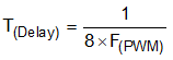
where
- F(PWM) is PWM dimming frequency set by PWMFREQ.