SLVSFZ4A December 2020 – February 2021 TPS929121-Q1
PRODUCTION DATA
- 1 Features
- 2 Applications
- 3 Description
- 4 Revision History
- 5 Device Comparison Table
- 6 Pin Configuration and Functions
- 7 Specifications
-
8 Detailed Description
- 8.1 Overview
- 8.2 Functional Block Diagram
- 8.3
Feature Description
- 8.3.1 Device Bias and Power
- 8.3.2 Constant Current Output
- 8.3.3 PWM Dimming
- 8.3.4 On-chip 8-bit Analog-to-Digital Converter (ADC)
- 8.3.5
Diagnostic and Protection in Normal State
- 8.3.5.1 Fault Masking
- 8.3.5.2 Supply Undervoltage Lockout Diagnostics in Normal State
- 8.3.5.3 Low-Supply Warning Diagnostics in Normal State
- 8.3.5.4 Reference Diagnostics in Normal State
- 8.3.5.5 Pre-Thermal Warning and Overtemperature Protection in Normal State
- 8.3.5.6 Communication Loss Diagnostic in Normal State
- 8.3.5.7 LED Open-Circuit Diagnostics in Normal State
- 8.3.5.8 LED Short-Circuit Diagnostics in Normal State
- 8.3.5.9 On-Demand Off-State Invisible Diagnostics
- 8.3.5.10 On-Demand Off-State Single-LED Short-Circuit (SS) Diagnostics
- 8.3.5.11 Automatic Single-LED Short-Circuit (AutoSS) Detection in Normal State
- 8.3.5.12 EEPROM CRC Error in Normal State
- 48
- 8.3.6
Diagnostic and Protection in Fail-Safe States
- 8.3.6.1 Fault Masking
- 8.3.6.2 Supply UVLO Diagnostics in Fail-Safe States
- 8.3.6.3 Low-supply Warning Diagnostics in Fail-Safe states
- 8.3.6.4 Reference Diagnostics at Fail-Safe States
- 8.3.6.5 Overtemperature Protection in Fail-Safe State
- 8.3.6.6 LED Open-circuit Diagnostics in Fail-Safe State
- 8.3.6.7 LED Short-circuit Diagnostics in Fail-Safe State
- 8.3.6.8 EEPROM CRC Error in Fail-safe State
- 58
- 8.4 Device Functional Modes
- 8.5 Programming
- 8.6 Register Maps
- 9 Application and Implementation
- 10Power Supply Recommendations
- 11Layout
- 12Device and Documentation Support
- 13Mechanical, Packaging, and Orderable Information
9.2.3 Detailed Design Procedure
STEP 1: Determine the architecture at system level.
Because MCU is located in a speared board to the LED boards, the CAN physical layer must be utilized for off-board long distance communication between LED driver boards and MCU board. The overall system block diagram is shown in Figure 9-2 and the typical schematic for 24 strings of LED board is shown in Figure 9-2. The pullup resistors for RX and TX interface may or may not be required, depending the model of the CAN transceiver. Normally the pullup resistor value for RX and TX must be about 10 kΩ. TI recommends putting a 4.7-µF ceramic capacitor on the VLDO output to keep the voltage stable. Because only one CAN transceiver is required per one PCB board, the CAN transceiver must only be powered by one LDO output of the TPS929121-Q1. DO NOT tie the LDO outputs for all TPS929121-Q1 in one PCB board. TI also recommends placing a 4.7-µF decoupling ceramic capacitor close to the SUPPLY pin of each TPS929121-Q1 to obtain good EMC performance.
STEP 2: Thermal analysis for the worst application conditions.
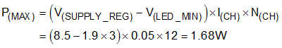
Normally the thermal analysis is necessary for linear LED-driver applications to ensure that the operation junction temperature of TPS929121-Q1 is well managed. The total power consumption on the TPS929121-Q1 itself is one important factor determining operation junction temperature, and it can be calculated by using Equation 8.

where
- V(SPPLY_MAX) is maximum supply voltage
- V(LED_MIN) is minimum output voltage
- I(CH) is channel current
- N(CH) is number of used channels
Based on the worst-case analysis for maximum power consumption on device, either optimizing PCB layout for better power dissipation as Layout Example describing or implementing a DC-to-DC converter in previous stage on MCU board can be considered. The DC-to-DC such as a buck converter or buck-boost converter can regulate the batter voltage to be a stable supply for the TPS929121-Q1 with sufficient headroom. It minimizes the power combustion on the TPS929121-Q1 itself as well as the whole system. In this application, the DC-to-DC converter with 8.5-V output voltage can make sure current output on each output channel of TPS929121-Q1 is stable. The calculated maximum power dissipation on the device is 1.68 W as Equation 9.
where
- V(SPPLY_MAX) is maximum supply voltage
- V(LED_MIN) is minimum output voltage
- I(CH) is channel current
- N(CH) is number of used channels
STEP 3: Set up the slave address for individual TPS929121-Q1.
The slave address of TPS929121-Q1 can be configured by ADDR2/ADDR1/ADDR0 pins or EEP_DEVADDR selected by EEP_INTADDR. The detail description is explained in UART Interface Address Setting. If the total number of TPS929121-Q1 is less than 8, TI recommends using ADDR2/ADDR1/ADDR0 pins for slave device configuration.
STEP 4: DC current setup for each LED string.
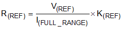
The DC current for all output channel can be programable by external resistor, R(REF) and internal register CONF_REFRANGE. The resistor value can be calculated by using Figure 9-2. The manufacturer default value for K(REF) is 512. If the other number rather than 512 is chosen for DC current setting, the selected code needs to burnt into EEPROM register EEP_REFRANGE to change the default value for CONF_REFRANGE. A 1-nF ceramic capacitor could be placed in parallel with R(REF) resistor to improve the noise immunity. The CONF_IOUTx register can be used to program DC current for each output channel independently mainly for dot correction purpose. The code setting for CONF_IOUTx must be decided in the end of production line according to the LED calibration result. The detail calculation is described in 64-Step Programmable High-Side Constat-Current Output.
where
- V(REF) = 1.235 V typically
- K(REF) = 64, 128, 256 or 512 (default)
| CURRENT (mA) | CONF_REFRANGE | K(REF) | REF RESISTOR VALUE (kΩ) |
|---|---|---|---|
| 50 | 11b | 512 | 12.7 |
| 10b | 256 | 6.34 | |
| 01b | 128 | 3.16 | |
| 00b | 64 | 1.58 |
TI recommends placing a 1-nF ceramic capacitor on each of output channels to achieve good EMC performance.
STEP 5: Design the configuration for PWM generator. Basically there are three main parameters for PWM generator must be considered including:
- PWM frequency set by CONF_PWMFREQ. The detail calculation and description is explained in PWM Dimming Frequency. The default value of CONF_PWMFREQ can be changed by burning the target value to EEP_PWMFREQ.
- PWM dutycycle set by CONF_PWMOUTx and CONF_PWMLOWOUTx. The detail calculation and description is explained in Linear Birhgtness Control. The default value of CONF_PWMOUTx can be changed by burning the target value to EEP_PWMFREQ.
- PWM dimming method set by CONF_EXPEN. The detail calculation and description is explained in Exponential Brightness Control. The default value of CONF_EXPEN can be changed by burning the target value to EEP_PWMFREQ.
STEP 6: Design the diagnostics configuration. The diagnostics configuration for both normal state and fail-safe states must be set up properly based on the system requirements. The following configuration registers need to designed:
- Low-supply warning threshold set by CONF_ADCLOWSUPTH. The detail calculation and description is explained in Low-Supply Warning Diagnostics in Normal State. The default value of CONF_ADCLOWSUPTH can be changed by burning the target value to EEP_ADCLOWSUPTH.
- Diagnostics enabling setup for each channel by CONF_DIAGENCHx. The diagnostics for each channel can be enabled or disabled by CONF_DIAGENCHx register. The detail description is explained in Fault Masking. The default value of CONF_DIAGENCHx can be changed by burning the target value to EEP_DIAGENCHx.
- On-demand invisible diagnostic current and pulse setup by CONF_ODIOUT and CONF_ODPW. The detail calculation and description is explained in On-Demand Off-State Invisible Diagnostics. The default value of CONF_ODIOUT and CONF_ODPW can be changed by burning the target value to EEP_ODIOUT and EEP_ODPW.
- Auto single-LED short-circuit configuration by CONF_AUTOSS and CONF_ADCSHORTTH. The detail calculation and description is explained in Automatic Single-LED Short-Circuit (AutoSS) Detection in Normal State. The default value of CONF_AUTOSS and CONF_ADCSHORTTH can be changed by burning the target value to EEP_AUTOSS and EEP_ADCSHORTTH.
- Fail-safe state access watchdog timer setup by CONF_WDTIMER. The detail calculation and description is explained in Normal State. The default value of CONF_WDTIME can be changed by burning the target value to EEP_WDTIMER.
- Channel setup in fail-safe states. Each output channels can be enabled or disabled independently in fail-safe state 0 and fail-safe state 1 by EEP_FS0CHx and EEPFS1CHx. In fail-safe state, the FS pin can be used as control signal to change device operating in fail-safe state 0 or fail-safe state 1. The manufacture defaults EEP_FS0CHx to 0 and EEP_FS1CHx to 1, so supply logic low voltage to FS pin turns off all the output channels in fail-safe state 0 and supply logic high voltage to FS pin turns on all the output channels in fail-safe state 1. With this configuration, input a PWM signal to FS pin can also achieve brightness control for all output channels. The detail calculation and description is explained in Fail-Safe States.
- One-fails-all-fail setup by EEP_OFAF. If the one-fails-all-fail can be enabled by burning 1 to EEP_OFAF according to system requirements. Tie the ERR pins for all TPS929121-Q1 in the system together with a single 4.7-kΩ pullup resistor to realize the one-fails-all-fail feature. The detail calculation and description is explained in Programmable Output Failure State.
- CRC check reference calculation for EEP_CRC. Once all EEPROM register data is designed, the CRC reference value for all EEPROM register needs to calculated and burnt into EEP_CRC. The detail calculation and description is explained in EEPROM CRC Error in Normal State.
STEP 7: EEPROM burning solution design.
TI recommends that the EEPROM burning be done in the end of production line; the detail flow is introduced in EEPROM Register Access and Burn .