ZHCSP77A December 2021 – March 2022 TPS92624-Q1
PRODUCTION DATA
- 1 特性
- 2 应用
- 3 说明
- 4 Revision History
- 5 Pin Configuration and Functions
- 6 Specifications
-
7 Detailed Description
- 7.1 Overview
- 7.2 Functional Block Diagram
- 7.3
Feature Description
- 7.3.1 Power Supply (SUPPLY)
- 7.3.2 Enable and Shutdown
- 7.3.3 Constant-Current Output and Setting (INx)
- 7.3.4 Thermal Sharing Resistor (OUTx and RESx)
- 7.3.5 PWM Control (PWMx)
- 7.3.6 Supply Control
- 7.3.7 Diagnostics
- 7.3.8 FAULT Bus Output With One-Fails-All-Fail
- 7.3.9 FAULT Table
- 7.3.10 LED Fault Summary
- 7.3.11 IO Pins Inner Connection
- 7.4 Device Functional Modes
- 8 Application and Implementation
- 9 Power Supply Recommendations
- 10Layout
- 11Device and Documentation Support
- 12Mechanical, Packaging, and Orderable Information
7.3.8 FAULT Bus Output With One-Fails-All-Fail
During normal operation, The FAULT pin of TPS92624-Q1 is weakly pulled up by an internal pullup current source, I(FAULT_pullup). If any fault scenario occurs, the FAULT pin is strongly pulled low by the internal pulldown current sink, I(FAULT_pulldown) to report out the fault alarm.
Meanwhile, the TPS92624-Q1 also monitors the FAULT pin voltage internally. If the FAULT pin of the TPS92624-Q1 is pulled low by external current sink below VIL(FAULT), the current output is turned off even though there is no fault detected on owned outputs. The device does not resume to normal operation until the FAULT pin voltage rises above VIH(FAULT).
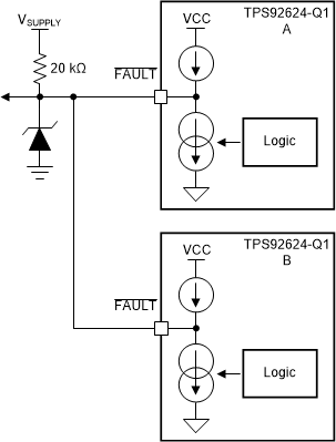
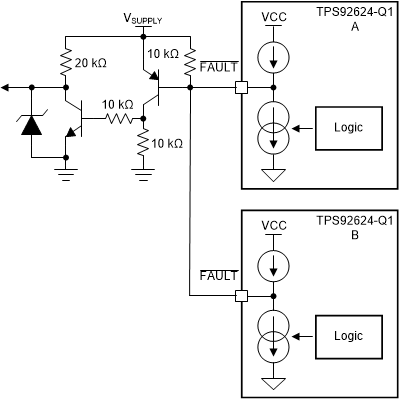
Based on this feature, the TPS92624-Q1 device is able to construct a FAULT bus by tying FAULT pins from multiple TPS92624-Q1 devices to achieve one-fails-all-fail function as Figure 7-6 showing. The lower side TPS92624-Q1 (B) detects any kind of LED fault and pulls low the FAULT pin. The low voltage on FAULT pin is detected by upper side TPS92624-Q1 (A) because the FAULT pins are connected of two devices. The upper side TPS92624-Q1 (A) turns off all output current for each channel as a result. If the FAULT pins of each TPS92624-Q1 are all connected to drive the base of an external PNP transistor as illustrated in Figure 7-7, the one-fails–all-fail function is disabled and only the faulty channel device is turned off.

