ZHCSJM3B April   2019  – January 2020 TPS92613-Q1

PRODUCTION DATA.  

  1. 特性
  2. 应用
  3. 说明
    1.     Device Images
      1.      典型应用图
  4. 修订历史记录
  5. Pin Configuration and Functions
    1.     Pin Functions
  6. Specifications
    1. 6.1 Absolute Maximum Ratings
    2. 6.2 ESD Ratings
    3. 6.3 Recommended Operating Conditions
    4. 6.4 Thermal Information
    5. 6.5 Electrical Characteristics
    6. 6.6 Timing Requirements
    7. 6.7 Typical Characteristics
  7. Detailed Description
    1. 7.1 Overview
    2. 7.2 Functional Block Diagram
    3. 7.3 Feature Description
      1. 7.3.1 Power Supply
        1. 7.3.1.1 Power-On Reset (POR)
        2. 7.3.1.2 Low-Quiescent-Current
      2. 7.3.2 Constant-Current Driver
      3. 7.3.3 PWM Control
      4. 7.3.4 Supply Control
      5. 7.3.5 Diagnostics and Protection
        1. 7.3.5.1 Open-Circuit Detection
        2. 7.3.5.2 Short-to-GND Detection
        3. 7.3.5.3 Overtemperature Protection
        4. 7.3.5.4 DIAGEN
        5. 7.3.5.5 Low-Dropout Operation
      6. 7.3.6 FAULT Bus Output With One-Fails–All-Fail
      7. 7.3.7 Fault Table
    4. 7.4 Device Functional Modes
      1. 7.4.1 Undervoltage Lockout, V(SUPPLY) < V(POR_rising)
      2. 7.4.2 Normal Operation V(SUPPLY) ≥ 4.5 V
      3. 7.4.3 Low-Voltage Dropout Operation
      4. 7.4.4 Fault Mode
  8. Application and Implementation
    1. 8.1 Application Information
    2. 8.2 Typical Applications
      1. 8.2.1 Single-Channel LED Driver With Diagnostics
        1. 8.2.1.1 Design Requirements
        2. 8.2.1.2 Detailed Design Procedure
        3. 8.2.1.3 Application Curves
      2. 8.2.2 Single-Channel LED Driver With Heat Sharing
        1. 8.2.2.1 Design Requirements
        2. 8.2.2.2 Detailed Design Procedure
        3. 8.2.2.3 Application Curves
  9. Power Supply Recommendations
  10. 10Layout
    1. 10.1 Layout Guidelines
    2. 10.2 Layout Example
  11. 11器件和文档支持
    1. 11.1 文档支持
      1. 11.1.1 相关文档
    2. 11.2 接收文档更新通知
    3. 11.3 支持资源
    4. 11.4 商标
    5. 11.5 静电放电警告
    6. 11.6 Glossary
  12. 12机械、封装和可订购信息

封装选项

机械数据 (封装 | 引脚)
散热焊盘机械数据 (封装 | 引脚)
订购信息

Pin Configuration and Functions

NDR Package
7-Pin TO-263 With Exposed Thermal Pad
Top View
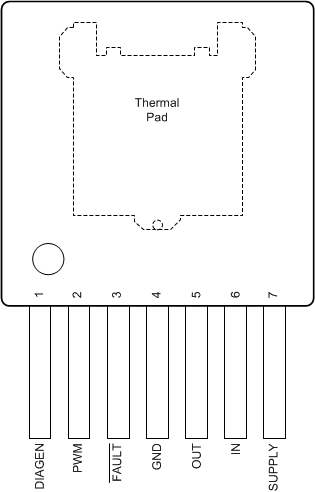
TPS92613-Q1 pinout-01-rgy-pkg-slvsec4.gif

Pin Functions

PIN I/O DESCRIPTION
NO. NAME
1 DIAGEN I Enable pin for LED open-circuit detection to avoid false open diagnostics during low-dropout operation
2 PWM I PWM input for current output ON/OFF control
3 FAULT I/O Fault output, support one-fails–all-fail fault bus
4 GND Ground
5 OUT O Constant-current output, connect to anode of the top LED in LED-string
6 IN I Current input
7 SUPPLY I Device supply voltage
Thermal pad Thermal pad, connect to ground