ZHCSJM3B April 2019 – January 2020 TPS92613-Q1
PRODUCTION DATA.
- 1 特性
- 2 应用
- 3 说明
- 4 修订历史记录
- 5 Pin Configuration and Functions
- 6 Specifications
- 7 Detailed Description
- 8 Application and Implementation
- 9 Power Supply Recommendations
- 10Layout
- 11器件和文档支持
- 12机械、封装和可订购信息
7.3.6 FAULT Bus Output With One-Fails–All-Fail
During normal operation, The FAULT pin of TPS92613-Q1 is weakly pulled up by an internal pullup current source, I(FAULT_pullup) higher than VOH(FAULT). If any fault scenario occurs, the FAULT pin is strongly pulled low by the internal pulldown current sink, I(FAULT_pulldown) to report out the fault alarm.
Meanwhile, the TPS92613-Q1 also monitors the FAULT pin voltage internally. If the FAULT pin of the TPS92613-Q1 is pulled low by external current sink below VIL(FAULT), the current output is turned off even though there is no fault detected on owned output. The device does not resume to normal operation until the FAULT pin voltage rises above VIH(FAULT).
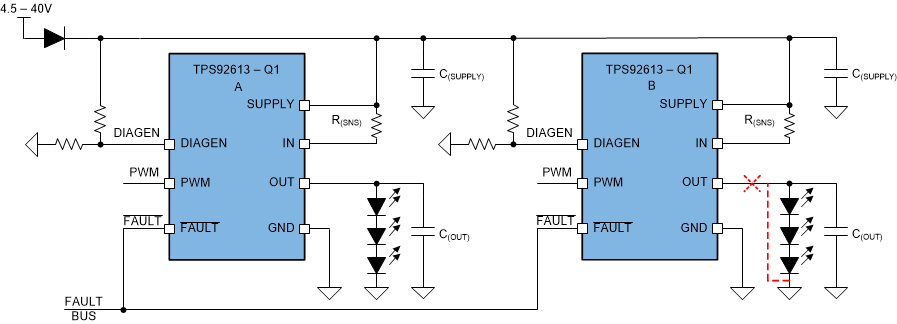
 Figure 22. Typical Application Schematic for One-Fails-All-Fail
 Based on this feature, the TPS92613-Q1 device is able to construct a FAULT bus by tying FAULT pins from multiple TPS9261x-Q1, TPS9263x-Q1 or TPS92830-Q1 devices to realize one-fails-all-fail function as Figure 22 showing. The right side TPS92613-Q1 (B) detects either LED open-circuit fault or LED short-to-GND fault and pulls low the FAULT pin. The low voltage on FAULT pin is detected by left side TPS92613-Q1 (A) because the FAULT pins are connected of two devices. The left TPS92613-Q1 (A) turns off the output current as a result.
If the FAULT pin is externally pulled up with a current larger than I(FAULT_pulldown), the one-fails–all-fail function is disabled and only the faulty channel is turned off.
The FAULT bus is able to support up to 15 pieces of TPS9261x-Q1, TPS9263x-Q1, or TPS92830-Q1 devices.