ZHCSJM3B April 2019 – January 2020 TPS92613-Q1
PRODUCTION DATA.
- 1 特性
- 2 应用
- 3 说明
- 4 修订历史记录
- 5 Pin Configuration and Functions
- 6 Specifications
- 7 Detailed Description
- 8 Application and Implementation
- 9 Power Supply Recommendations
- 10Layout
- 11器件和文档支持
- 12机械、封装和可订购信息
8.2.2.2 Detailed Design Procedure
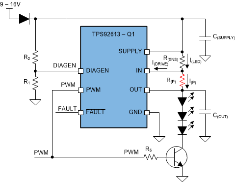
Note that the parallel resistor path cannot be shut down by PWM or fault protection. If PWM control is required, TI recommends an application circuit as described in Figure 27.
In linear LED driver applications, the large input voltage variation generates the most of the thermal concerns. The resistor current, as indicated by Ohm's law, depends on the voltage across the external resistors. The TPS92613-Q1 controls the driver current I(DRIVE) to attain the desired total current. If I(P) increases, the TPS92613-Q1 device decreases I(DRIVE) to compensate, and vice versa.
While in low-dropout operation, the voltage across the R(P) resistor may be close to zero, so that almost no current can flow through the external resistor R(P).
When the input voltage is high, the parallel-resistor current I(P) is proportional to the voltage across the parallel resistor R(P). The parallel resistor R(P) takes the majority of the total string current, generating maximum heat.
In this case, the parallel resistor value must be carefully calculated to ensure that 1) enough output current is achieved in low-dropout operation, 2) thermal dissipation for both the TPS92613-Q1 device and the resistor is within their thermal dissipation limits, and 3) device current in the high-voltage mode is above the minimal output-current requirement.
STEP 1: Determine the current setting resistor, R(SNS) value by using Equation 5.

where
- V(CS_REG) = 98 mV (typical)
- I(LED) = 500 mA
The calculated result for R(SNS) is 0.196 Ω.
STEP 2: Calculate the parallel resistor, R(P) value by using Equation 6.
The parallel resistor R(P) is recommended to consume 50% of the total current at maximum supply voltage.

where
- V(CS_REG) = 98 mV (typical)
- I(LED) = 500 mA
The calculated result for R(P) is about 40 Ω at V(SUPPLY) = 16 V.
STEP 3: Design the threshold voltage for SUPPLY to enable the LED open-circuit diagnostics and calculate voltage divider resistor value for R1 and R2.
LED-string maximum forward voltage = 3 × 2.5 V = 7.5 V. To avoid the open-circuit fault reported in low-dropout operation conditions, additional headroom between SUPPLY and OUT needs to be considered. The TPS92613-Q1 device must disable open-circuit detection when the supply voltage is below LED-string maximum forward voltage plus maximum V(OPEN_th_rising) and maximum V(CS_REG). The voltage divider resistor, R1 and R2 value can be calculated by Equation 7.

where
- VIL(DIAGEN) = 1.045 V (minimum)
- V(OPEN_th_rising) = 335 mV (maximum)
- V(CS_REG) = 102.5 mV (maximum)
- R1 = 10 kΩ recommended
The calculated result for R2 is 65.7 kΩ when V(OUT) maximum voltage is 7.5 V.
STEP 4: Design the threshold voltage for PWM to enable current output and calculate voltage divider resistor value for R3 and R4.
Because the supply control is adopted for the LED ON/OFF and brightness control, a pulse square voltage with power capability is applied on the SUPPLY pin to enable and disable current output to OUT. In order to ensure the current output of TPS92613-Q1 is fully enabled when applied voltage on SUPPLY pin is high enough and the current output is truly shutdown when the applied voltage goes low. A voltage divider from supply to control PWM needs to be designed to setup a threshold of supply voltage. The resistor R3 and R4 of voltage divider can be calculated by Equation 8.

where
- VIL(PWM) = 1.24 V (maximum)
- R3 = 10 kΩ recommended
The calculated result for R4 is 30.5 kΩ if LED must be turned on when V(SUPPLY) voltage is higher than 5 V.
STEP 5: Thermal analysis for the worst application conditions.
The total device power consumption can be calculated by Equation 9.

where
- V(CS_REG) = 98 mV (typical)
- I(Quiescent) = 250 µA (maximum)
The calculated maximum power consumption on the TPS61193-Q1 is 2.5 W at V(SUPPLY) = 16 V, V(OUT) = 3 × 1.9 V = 5.7 V and I(LED) = 500 mA.
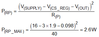
The power consumption on resistor R(P) can be calculated through Equation 10.

where
- V(CS_REG) = 98 mV (Typ.)
The calculated maximum power consumption on the 40 Ω, R(P) parallel resistor is 2.6 W at V(SUPPLY) = 16 V and V(OUT) = 3 × 1.9 V = 5.7 V.
TI recommends adding capacitors C(SUPPLY) at SUPPLY and C(OUT)at OUT. One 1-μF capacitor plus one 100-nF decoupling ceramic capacitor close to the SUPPLY pin is recommended for C(SUPPLY), and a 10-nF ceramic capacitor close to the OUT pin is recommended for C(OUT). The larger capacitor for C(SUPPLY) or C(OUT) is helpful for EMI and ESD immunity, however large C(OUT) takes a longer time to charge up the capacitor and could affect PWM dimming performance.
 Figure 27. PWM Control With Heat Sharing Resistor
 For PWM control scenarios, a NPN bipolar transistor with a base current-limiting resistor, R5 can modulate the output current together with the device PWM function as Figure 27. The resistor value of R5 needs to be calculated based on the applied PWM voltage and β value of selected NPN transistor.