ZHCSC49A March 2014 – May 2014 TPS92511
PRODUCTION DATA.
- 1 特性
- 2 应用范围
- 3 说明
- 4 修订历史记录
- 5 Pin Configuration and Functions
- 6 Specifications
-
7 Detailed Description
- 7.1 Overview
- 7.2 Functional Block Diagram
- 7.3
Feature Description
- 7.3.1 Pulse Level Modulation (PLM) Control
- 7.3.2 Pulse Level Modulation (PLM) Operaion Principles
- 7.3.3 PLM Control enable Common-Anode Low-Side Sensing (CALS)Technique to Save Wiring
- 7.3.4 Internal Regulator
- 7.3.5 Setting The Switching Frequency
- 7.3.6 Setting The LED Current
- 7.3.7 Integrated MOSFET
- 7.3.8 Inductor Selection
- 7.3.9 Integrated MOSFET Current Limit
- 7.3.10 PWM Dimming Control
- 7.3.11 Analog Dimming
- 7.3.12 High Voltage Buck Configuration
- 7.3.13 Thermal Foldback
- 7.3.14 EMI Consideration
- 7.4 Device Functional Modes
- 8 Application and Implementation
- 9 Power Supply Recommendation
- 10Layout
- 11器件和文档支持
- 12机械封装和可订购信息
8 Application and Implementation
8.1 Application Information
The TPS92511 is an LED driver which provides a regulated output current to drive a single string of LED with the forward voltage lower than the input voltage. The following procedures design a TPS92511 application circuit with an input voltage of 48V, driving an LED string of 38V at an LED current of 0.5A. The switching frequency is 300 kHz.
8.2 Typical Application
8.2.1 TPS92511 LED driver for 12 LEDs at 0.5A
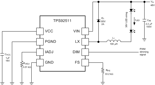 Figure 23. Application Circuit of TPS92511 (fSW = 300 kHz and ILED = 0.5A)
8.2.1.1 Design Requirements
Table 4. Design Parameters
| DESIGN PARAMETER | EXAMPLE VALUE |
|---|---|
| Input voltage range | 43V to 53V |
| LED current | 0.5A |
| LED string forward voltage | 38V |
| Operating frequency | 300 kHz |
8.2.1.2 Detailed Design Procedure
CIN: The function of the input capacitor CIN is to reduce the input voltage ripple. Ceramic capacitors are recommended owing to the concern of product lifetime. A 100V 2.2 µF ceramic capacitor is selected in this circuit.
CVCC: The capacitor on the VCC pin provides noise filtering and stabilizes the internal regulator. It also prevents false triggering of the VCC UVLO. CVCC is recommended to be a 1 μF good quality and low ESR ceramic capacitor.
D1: The diode D1 should have a reverse voltage larger than VIN in the floating buck topology. In this circuit, a 100V diode is selected.
RFS and RIADJ: In this circuit, the switching frequency and LED current are designed to be 300 kHz and 0.5A. From Table 1 and Table 2, RFS is 33.2 kΩ and RIADJ is 3.01 kΩ.
L1: The selection of inductor mainly affects the inductor current ripple. In this circuit, we design the peak to peak inductor current ripple to be 50% of ILED, i.e. 0.25A. From (6), L1 is calculated to be 106 µH, and a 100 µH inductor is selected.
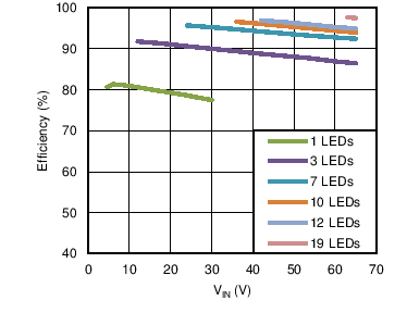
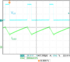
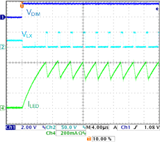
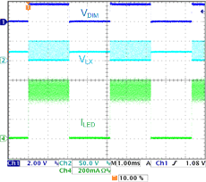
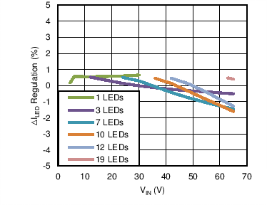
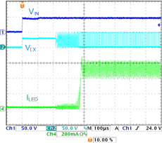
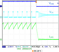
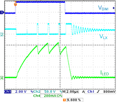
8.2.1.3 Application Curves