ZHCSC49A March 2014 – May 2014 TPS92511
PRODUCTION DATA.
- 1 特性
- 2 应用范围
- 3 说明
- 4 修订历史记录
- 5 Pin Configuration and Functions
- 6 Specifications
-
7 Detailed Description
- 7.1 Overview
- 7.2 Functional Block Diagram
- 7.3
Feature Description
- 7.3.1 Pulse Level Modulation (PLM) Control
- 7.3.2 Pulse Level Modulation (PLM) Operaion Principles
- 7.3.3 PLM Control enable Common-Anode Low-Side Sensing (CALS)Technique to Save Wiring
- 7.3.4 Internal Regulator
- 7.3.5 Setting The Switching Frequency
- 7.3.6 Setting The LED Current
- 7.3.7 Integrated MOSFET
- 7.3.8 Inductor Selection
- 7.3.9 Integrated MOSFET Current Limit
- 7.3.10 PWM Dimming Control
- 7.3.11 Analog Dimming
- 7.3.12 High Voltage Buck Configuration
- 7.3.13 Thermal Foldback
- 7.3.14 EMI Consideration
- 7.4 Device Functional Modes
- 8 Application and Implementation
- 9 Power Supply Recommendation
- 10Layout
- 11器件和文档支持
- 12机械封装和可订购信息
7 Detailed Description
7.1 Overview
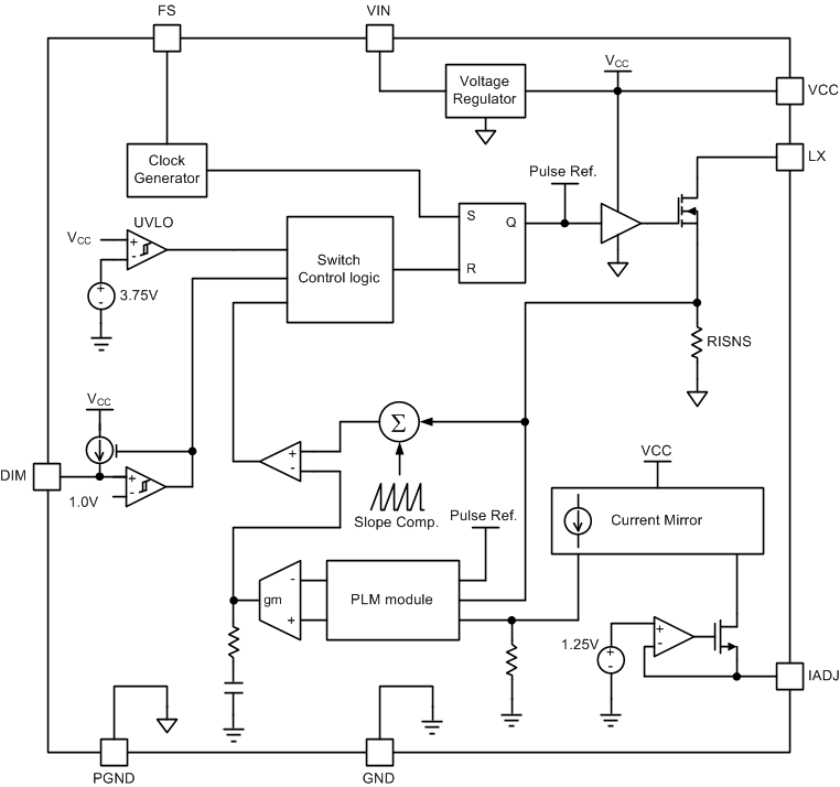
The TPS92511 is an easy to use constant current buck converter for driving a single LED string with current up to 0.5A and efficiency up to 95%. Only 5 external components are required for basic operation and single layer PCB layout is feasible because of the integration of a N-MOSFET, no external current sensing resistor, no external compensation and the proper pin assignment. A high-value external resistor programs the LED current so that fine tuning of the LED current can be achieved. Another high-value external resistor programs a constant switching frequency from 50kHz to 500kHz. As a result of constant switching frequency, EMI design becomes easy. The TPS92511 provides a wide input voltage range from 4.5V to 65V. By adding simple external circuits, it can handle applications with even higher input voltages.
The TPS92511 employs a proprietary Pulse-Level-Modulation (PLM) control scheme under continuous conduction mode (CCM) to regulate the LED current without the need of sensing the LED current directly. It applies a floating buck topology with a low-side N-channel power MOSFET, which does not need boot-strapping capacitor, so that driving LED string under drop-out conditions and very high input voltages are feasible. For multiple channel systems, the floating buck topology without external current sensing network together with the proprietary control scheme allows a common-anode connection of the LED strings without external current sensing network. This saves high-side current sensing wirings for separate driver boards and LED board systems and significantly reduces the number of wiring, which can lower overall manufacturing cost.
The TPS92511 has very fast PWM dimming response time. There is almost no delay between the DIM pin voltage rising edge and the start of the LED current conduction, so it can dim down to nearly zero current. In order to maintain good dimming linearity, the minimum LED current pulse width is suggested to be three switching cycles. For example, if the switching frequency is 500 kHz, the minimum DIM pulse width is 6µs and the dimming frequency is 150Hz, a contrast ratio of more than 1000:1 can be achieved.
7.2 Functional Block Diagram
7.3 Feature Description
7.3.1 Pulse Level Modulation (PLM) Control
A proprietary Pulse-Level-Modulation (PLM) control method is used in the TPS92511. It can regulate the average LED current by sensing only the inductor current at the on-period (Figure 13). The integrated MOSFET and the sensing and control circuits in the TPS92511 implement the whole PLM control internally so the control does not suffer from tolerance and noise issues that may be coming from external components. As compared with the conventional method which regulates average LED current by sensing the current over the entire switching cycle, the power dissipation on the sensing circuit in PLM is much lower. For example, consider a duty cycle of 0.5, the power dissipation on current sensing in PLM can be reduced by half. PLM requires no external loop compensation circuit. Besides, the accuracy of the regulated LED current is high (typically ±3.5% in the TPS92511).
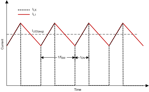 Figure 13. Waveforms of a Floating Buck LED Driver with PLM
7.3.2 Pulse Level Modulation (PLM) Operaion Principles
The Pulse-Level-Modulation is a patented method to ensure an accurate average output current regulation without the need of direct output current sensing. Figure 13 shows the current waveforms of a typical buck converter under steady state, where, IL1 is the inductor current and ILX is the current flowing into the LX pin. For a buck converter operating in steady state, the mid-point of the RAMP portion of IL1 equals to the average value of IL1 and hence the average LED current ILED(avg). In short, by regulating the mid-point with respect to a precise reference level, PLM achieves LED current regulation by sensing the main MOSFET current solely, instead of the entire cycle of IL1.
7.3.3 PLM Control enable Common-Anode Low-Side Sensing (CALS)Technique to Save Wiring
For multi-channel systems with separated driver boards and LED array boards, the Pulse-Level-Modulation (PLM) control scheme enable Common-Anode Low-Side Current Sensing to save inter-board wirings. Figure 14 shows a conventional configuration with a Low-side switching and High-Side Current Sensing. For an n channel system with separated driver and an LED array boards, 2n inter-board wirings are required. For example, an 128-channel system needs 256 inter-board wirings, which implies a high material and manufacturing cost. Figure 15 shows the PLM configuration with Low-side switching and Low-Side Current Sensing. A Common-Anode configuration is used for the LED array board. As shown in the figure, an n channel system with separated driver and LED array boards requires only n+1 inter-board wirings. For an 128-channel system, only 129 inter-board wirings are required. The wiring cost is cut by half, and the cost of the end product can be reduced.
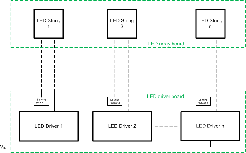 Figure 14. Conventional Configuration with Low-Side Switching and High-Side Current Sensing Requires 2×n Inter-Board Wirings
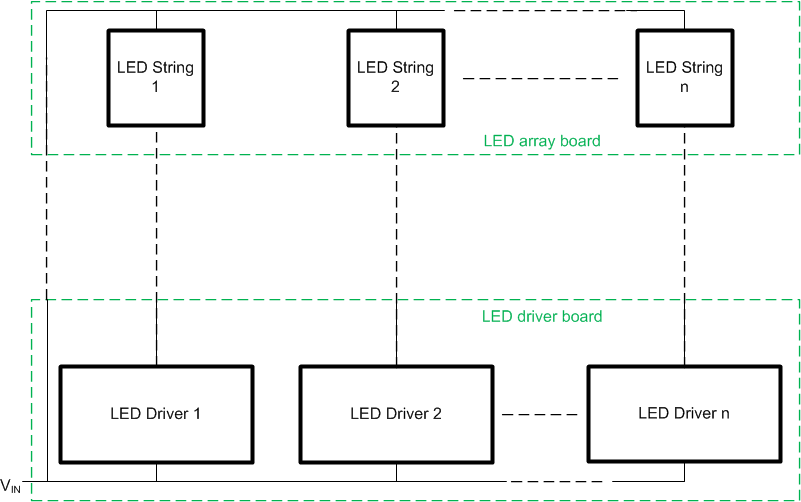 Figure 15. PLM Configuration with Common-Anode Low-Side Switching Requires n+1 Inter-Board Wirings
7.3.4 Internal Regulator
The TPS92511 integrates an internal voltage regulator for powering internal circuitry. For stability, an external capacitor CVCC of at least 1 μF should be connected between the VCC and PGND pins The output of the internal regulator VCC is 5.4V when VIN is larger than 6V. If VIN is lower than 6V, VCC decreases. The TPS92511 will trigger the VCC under-voltage lock-out if VCC falls below typically 3.5V. VCC can be used to bias external circuits subject to a loading of maximum 2 mA, while it has a short circuit current limit at typically 16 mA.
7.3.5 Setting The Switching Frequency
The switching frequency fSW of the TPS92511 is programmable in the range of 50 kHz to 500 kHz by a single resistor RFS connecting the FS pin and ground. The following equation shows the relationship between fSW and RFS:
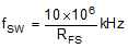
Figure 16 plots fsw against RFS. Table 1 shows values of RFS for commonly used switching frequencies.
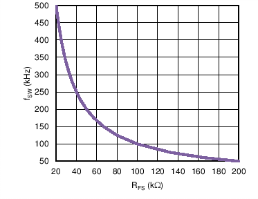 Figure 16. Switching Frequency vs RFS
Table 1. Commonly Used fSW And RFS
| fSW (kHz) | RFS (kΩ) |
|---|---|
| 50 | 200 |
| 100 | 100 |
| 300 | 33.2 |
| 500 | 20 |
7.3.6 Setting The LED Current
The LED current ILED of the TPS92511 is programmable by a single resistor RIADJ connecting the IADJ pin and ground. The IADJ pin is internally biased to 1.25 V. Equation 2 shows the relationship between ILED and RIADJ:

To ensure stability, RIADJ must be less that 30 kΩ, implying a minimum ILED of 50 mA can be programmed. The tolerance of ILED of 150 mA is shown in the ELECTRICAL CHARACTERISTICS. Larger tolerance should be expected for lower ILED. Figure 17 plots ILED against RIADJ. Table 2 shows values of RIADJ for commonly used ILED.
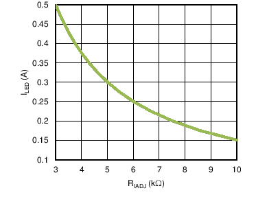 Figure 17. LED Current vs RIADJ
Table 2. Commonly Used ILED And RIADJ
| ILED (mA) | RIADJ (kΩ) |
|---|---|
| 150 | 10 |
| 350 | 4.32 |
| 500 | 3.01 |
7.3.7 Integrated MOSFET
The TPS92511 integrates a N-channel power MOSFET, the drain of which is connected to the LX pin. When the integrated MOSFET is turned on, the resistance across the LX and GND pins is typically 1.4Ω. The integrated MOSFET has a fixed current limit of 1.2A to protect the application circuit during critical operation conditions like short circuit of the LED string. Once the limit is hit, the integrated MOSFET turns off immediately for 34 µs to let the inductor discharge.
The minimum on-time of the integrated MOSFET is 400 ns. It may be hit at a high switching frequency and a high VIN/VLED ratio. Once hit, the ILED regulation may be affected. In the worst case, ILED may be boost up to a level higher than the programmed value, and the LED string and/or the inductor may be damaged as a result. Hence, it is recommened that the ratio between VIN and VLED should be designed under the following constraint:
7.3.8 Inductor Selection
Operating in the continuous conduction mode (CCM) is required in the TPS92511 application circuit. In the CCM, considering the on-period, the peak-to-peak inductor current ripple (2ΔIL1) is shown in Equation 4.
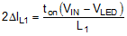
Because

L1 can be a function of VIN, VLED, fSW and ΔIL1 as shown in Equation 6 .
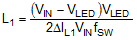
The value of L1 is selected by designers with the consideration of all above parameters. The minimum L1 calculated by the following equation is a good starting point for designing L1:
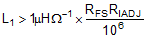
The following table shows some typical examples of using RFS and RIADJ to estimate the minimum L1:
Table 3. Estimation Of Minimum L1 Using RFS And RIADJ
| RFS (kΩ) | RIADJ (kΩ) | Estimated Minimum L1 (µH) | Recommended L1 (µH) |
|---|---|---|---|
| 100 | 10 | 1000 | 1000 |
| 33.2 | 3.01 | 100 | 100 |
| 20 | 4.32 | 86 | 100 |
| 20 | 3.01 | 60 | 68 |
To maintain the CCM, ΔIL1 must be smaller than the average LED current ILED(avg). Hence, the minimum inductance used is:
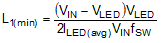
In the absence of output capacitors, the TPS92511 can maintain a continuous ILED throughout the entire switching cycle because in such case the inductor current is the same as ILED (floating buck topology operating in the CCM). However, the LED peak current must not exceed the rated current of the LED. The peak LED current can be found by the following equation:
7.3.9 Integrated MOSFET Current Limit
The current limit of the integrated MOSFET is internally fixed at 1.2A to protect the LED string, the inductor and the integrated MOSFET from overdriven. Once triggered, the integrated MOSFET turns off immediately for 34 µs to let the inductor to discharge. The triggering of the current limit cycles repetitively until all overdriven conditions disappear.
7.3.10 PWM Dimming Control
The TPS92511 implements PWM dimming by applying a PWM dimming signal to the DIM pin. A low input applying to the DIM pin disables the switching of the integrated MOSFET, and as a result discharges the inductor and then turns off the LED string. To turn on the LED string, the DIM pin should be connected to high or left open (since it is internally pulled high by a current of typically 40 µA and 90 µA when the DIM pin is low and high respectively). The PWM dimming frequency is recommended to be lower than 0.1fSW to ensure normal operation.
7.3.11 Analog Dimming
Analog dimming can be implemented by injecting a current to RIADJ (Figure 18) and as a result reduces the current of the IADJ pin, IADJ, which is controlled internally by the TPS92511 to bias the voltage on the IADJ pin to be 1.25V. If the CCM can be maintained, the minimum IADJ can achieve 15 µA, which refers to an ILED of 18 mA. If IADJ is further decreased, ILED may not follow due to the presence of the minimum on-time of the integrated MOSFET. If the CCM cannot be maintained, ILED can still decrease monotonically with IADJ. However, if good line and load regulations are required, the CCM should be maintained by using a large inductance.
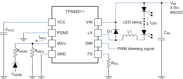 Figure 18. Circuit Configuration for Analog Dimming
7.3.12 High Voltage Buck Configuration
The TPS92511 can handle applications with an input voltage higher than 65V, which is the maximum VIN of the recommended operating condition of the TPS92511, by adding an external high voltage N-channel MOSFET to the application circuit as shown in Figure 19. PWM dimming can be implemented in this circuit without additional efforts, and analog dimming is also feasible by referencing to additional circuits shown in Figure 18.
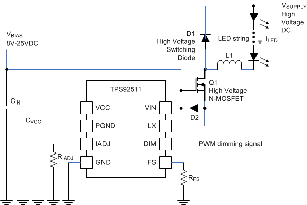 Figure 19. Circuit Configuration for Very High Voltage Buck
7.3.13 Thermal Foldback
Thermal foldback is useful to prevent over-temperature of LEDs during operation by sensing the temperature of LEDs and, if the sensed temperature is high, reducing ILED to decrease the power and as well as the temperature of LEDs. Thanks to the feature of analog dimming, thermal foldback can be implemented by embedding a negative temperature coefficient (NTC) resistor, RNTC, into a circuit as shown in Figure 20. When the sensed temperature increases, RNTC decreases and thus the emitter current of QT1 increases to reduce ILED by means of analog dimming. The resistor RTF can adjust the loop gain of the thermal foldback control loop, which should be high enough to avoid oscillation and maintain stability.
 Figure 20. Circuit Configuration for Thermal Foldback
7.3.14 EMI Consideration
Conductive and radiative EMI can be major concerns for lighting applications. The TPS92511 application circuit can be designed for the EN 55022 class B standard by adding a few external components, as shown in Figure 21. The input filter which consists of an inductor L2 and two capacitors CIN2 and CIN3 takes care of the conductive EMI, while the output capacitor CLED and the ferrite bead FB1 which inserts between the LX pin and D1 take care of the radiative EMI.
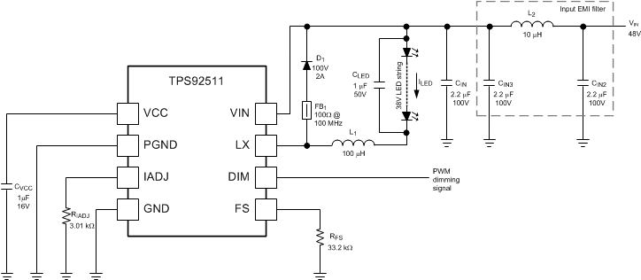 Figure 21. Circuit Configuration with EMI Design Consideration
7.4 Device Functional Modes
7.4.1 Operation with VIN < 4.5 V (minimum VIN)
For the typical application circuit, when the input voltage drops so that the VCC voltage regulator is under drop-out mode, and the VCC voltage drops below the “VCC UVLO Lower Threshold” (typically 3.48V), the switching of the main MOSFET is stopped, and the LED current will become zero. At the same time, the voltages of both the FS and IADJ pins will become zero .
When the input voltage increases from zero and the VCC voltage is increased to cross over the “VCC UVLO Upper Threshold” (typically 3.75V), the voltages on the FS and IADJ pins will rise to their regulation voltage (typically 1.25V), the switching of the main MOSFET is started upon the DIM pin voltage is HIGH, and the LED current will ramp up to its preset value set by RIADJ.
7.4.2 Operation with DIM control
For the typical application circuit, when the VCC voltage is not under UVLO condition, the switching of the main MOSFET is enabled and the LED current is conducted if the DIM pin voltage is higher than the “DIM Pin Upper Threshold” (typically 1V).
Alternaltively, the switching is disabled and the LED current is cut off if the voltage of the DIM pin is lower than the “DIM Pin Lower Threshold” (typically 0.675V).
7.4.3 Linear Mode
When the VCC voltage is not under UVLO condition and the voltage on the FS pin is forced to be higher than 4.2V but lower than 5V, the switching of the main MOSFET is disabled, and the TPS92511 is working in the Linear Mode. In the Linear Mode, if the voltage on the DIM pin is higher than the “DIM Pin Upper Threshold” (typically 1V), the TPS92511 will regulate the LX pin in-going current according to the preset value set by RIADJ. Alternatively, if the voltage on the DIM pin is lower than the “DIM Pin Lower Threshold” (typically 0.675V), the LX pin will open and its in-going current will become zero.
Below is the simple configuration to have the TPS92511 working as a linear current shunt regulator.
 Figure 22. Circuit Configuration for Working as a Linear Current Shunt Regulator