ZHCSH45B June 2017 – October 2021 TPS7A83A
PRODUCTION DATA
- 1 特性
- 2 应用
- 3 说明
- 4 Revision History
- 5 说明(续)
- 6 Pin Configuration and Functions
-
7 Specifications
- 7.1 Absolute Maximum Ratings
- 7.2 ESD Ratings
- 7.3 Recommended Operating Conditions
- 7.4 Thermal Information
- 7.5 Electrical Characteristics: General
- 7.6 Electrical Characteristics: TPS7A8300A
- 7.7 Electrical Characteristics: TPS7A8301A
- 7.8 Typical Characteristics: TPS7A8300A
- 7.9 Typical Characteristics: TPS7A8301A
- 8 Detailed Description
-
9 Application and Implementation
- 9.1
Application Information
- 9.1.1
External Component Selection
- 9.1.1.1 Adjustable Operation
- 9.1.1.2 ANY-OUT Programmable Output Voltage
- 9.1.1.3 ANY-OUT Operation
- 9.1.1.4 Increasing ANY-OUT Resolution for LILO Conditions
- 9.1.1.5 Recommended Capacitor Types
- 9.1.1.6 Input and Output Capacitor Requirements (CIN and COUT)
- 9.1.1.7 Feed-Forward Capacitor (CFF)
- 9.1.1.8 Noise-Reduction and Soft-Start Capacitor (CNR/SS)
- 9.1.2 Start Up
- 9.1.3 AC and Transient Performance
- 9.1.4 DC Performance
- 9.1.5 Sequencing Requirements
- 9.1.6 Negatively Biased Output
- 9.1.7 Reverse Current
- 9.1.8 Power Dissipation (PD)
- 9.1.1
External Component Selection
- 9.2 Typical Application
- 9.1
Application Information
- 10Power Supply Recommendations
- 11Layout
- 12Device and Documentation Support
- 13Mechanical, Packaging, and Orderable Information
封装选项
机械数据 (封装 | 引脚)
散热焊盘机械数据 (封装 | 引脚)
订购信息
9.1.4.2 Dropout Voltage (VDO)
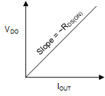
Generally speaking, dropout voltage often refers to the minimum voltage difference between the input and output voltage (VDO = VIN – VOUT) that is required for regulation. When VIN drops below the required VDO for the given load current, the device functions as a resistive switch and does not regulate output voltage. Figure 9-11 shows that dropout voltage is proportional to the output current because the device is operating as a resistive switch.
 Figure 9-11 Dropout Voltage versus Output Current
Dropout voltage is affected by the drive strength for the gate of the pass element, which is nonlinear with respect to VIN on this device because of the internal charge pump. Dropout voltage increases exponentially when the input voltage nears its maximum operating voltage.