ZHCSH45B June 2017 – October 2021 TPS7A83A
PRODUCTION DATA
- 1 特性
- 2 应用
- 3 说明
- 4 Revision History
- 5 说明(续)
- 6 Pin Configuration and Functions
-
7 Specifications
- 7.1 Absolute Maximum Ratings
- 7.2 ESD Ratings
- 7.3 Recommended Operating Conditions
- 7.4 Thermal Information
- 7.5 Electrical Characteristics: General
- 7.6 Electrical Characteristics: TPS7A8300A
- 7.7 Electrical Characteristics: TPS7A8301A
- 7.8 Typical Characteristics: TPS7A8300A
- 7.9 Typical Characteristics: TPS7A8301A
- 8 Detailed Description
-
9 Application and Implementation
- 9.1
Application Information
- 9.1.1
External Component Selection
- 9.1.1.1 Adjustable Operation
- 9.1.1.2 ANY-OUT Programmable Output Voltage
- 9.1.1.3 ANY-OUT Operation
- 9.1.1.4 Increasing ANY-OUT Resolution for LILO Conditions
- 9.1.1.5 Recommended Capacitor Types
- 9.1.1.6 Input and Output Capacitor Requirements (CIN and COUT)
- 9.1.1.7 Feed-Forward Capacitor (CFF)
- 9.1.1.8 Noise-Reduction and Soft-Start Capacitor (CNR/SS)
- 9.1.2 Start Up
- 9.1.3 AC and Transient Performance
- 9.1.4 DC Performance
- 9.1.5 Sequencing Requirements
- 9.1.6 Negatively Biased Output
- 9.1.7 Reverse Current
- 9.1.8 Power Dissipation (PD)
- 9.1.1
External Component Selection
- 9.2 Typical Application
- 9.1
Application Information
- 10Power Supply Recommendations
- 11Layout
- 12Device and Documentation Support
- 13Mechanical, Packaging, and Orderable Information
封装选项
机械数据 (封装 | 引脚)
散热焊盘机械数据 (封装 | 引脚)
订购信息
9.1.8.1 Estimating Junction Temperature
The JEDEC standard now recommends the use of psi (Ψ) thermal metrics to estimate the junction temperatures of the LDO when in-circuit on a typical PCB board application. These metrics are not strictly speaking thermal resistances, but rather offer practical and relative means of estimating junction temperatures. These psi metrics are determined to be significantly independent of the copper-spreading area. The key thermal metrics (ΨJT and ΨJB) are used in accordance with Equation 14.
Equation 14. 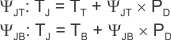
where:
- PD is the power dissipated as explained in Equation 11
- TT is the temperature at the center-top of the device package, and
- TB is the PCB surface temperature measured 1 mm from the device package and centered on the package edge