ZHCSK49E August   2019  – September 2022 TPS7A24

PRODUCTION DATA  

  1. 特性
  2. 应用
  3. 说明
  4. Revision History
  5. Pin Configuration and Functions
  6. Specifications
    1. 6.1 Absolute Maximum Ratings
    2. 6.2 ESD Ratings
    3. 6.3 Recommended Operating Conditions
    4. 6.4 Thermal Information
    5. 6.5 Electrical Characteristics
    6. 6.6 Typical Characteristics
  7. Detailed Description
    1. 7.1 Overview
    2. 7.2 Functional Block Diagrams
    3. 7.3 Feature Description
      1. 7.3.1 Output Enable
      2. 7.3.2 Dropout Voltage
      3. 7.3.3 Current Limit
      4. 7.3.4 Undervoltage Lockout (UVLO)
      5. 7.3.5 Thermal Shutdown
      6. 7.3.6 Active Overshoot Pulldown Circuitry
    4. 7.4 Device Functional Modes
      1. 7.4.1 Device Functional Mode Comparison
      2. 7.4.2 Normal Operation
      3. 7.4.3 Dropout Operation
      4. 7.4.4 Disabled
  8. Application and Implementation
    1. 8.1 Application Information
      1. 8.1.1 Adjustable Device Feedback Resistors
      2. 8.1.2 Recommended Capacitor Types
      3. 8.1.3 Input and Output Capacitor Requirements
      4. 8.1.4 Reverse Current
      5. 8.1.5 Feed-Forward Capacitor (CFF)
      6. 8.1.6 Power Dissipation (PD)
      7. 8.1.7 Estimating Junction Temperature
      8. 8.1.8 Special Consideration for Line Transients
    2. 8.2 Typical Application
      1. 8.2.1 Design Requirements
      2. 8.2.2 Detailed Design Procedure
        1. 8.2.2.1 Transient Response
        2. 8.2.2.2 Selecting Feedback Divider Resistors
        3. 8.2.2.3 Thermal Dissipation
      3. 8.2.3 Application Curve
    3. 8.3 Power Supply Recommendations
    4. 8.4 Layout
      1. 8.4.1 Layout Guidelines
      2. 8.4.2 Layout Examples
  9. Device and Documentation Support
    1. 9.1 Device Support
      1. 9.1.1 Device Nomenclature
    2. 9.2 接收文档更新通知
    3. 9.3 支持资源
    4. 9.4 Trademarks
    5. 9.5 Electrostatic Discharge Caution
    6. 9.6 术语表
  10. 10Mechanical, Packaging, and Orderable Information

封装选项

机械数据 (封装 | 引脚)
散热焊盘机械数据 (封装 | 引脚)
订购信息

Special Consideration for Line Transients

During a line transient, the response of this LDO to a very large or fast input voltage change can cause a brief shutdown lasting up to a few hundred microseconds from the voltage transition. This shutdown can be avoided by reducing the voltage step size, increasing the transition time, or a combination of both. Figure 8-3 provides a boundary to follow to avoid this behavior. If necessary, reduce slew rate and the voltage step size to stay below the curve.
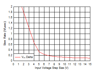
GUID-3EDFA866-E1DA-453E-BD60-CC39F6411DF7-low.gifFigure 8-3 Recommended Input Voltage Step and Slew Rate in a Line Transient