ZHCSN51J june   2007  – april 2023 TPS74901

PRODUCTION DATA  

  1. 特性
  2. 应用
  3. 说明
  4. Revision History
  5. Pin Configuration and Functions
  6. Specifications
    1. 6.1  Absolute Maximum Ratings
    2. 6.2  ESD Ratings
    3. 6.3  Recommended Operating Conditions
    4. 6.4  Thermal Information
    5. 6.5  Electrical Characteristics: Other Orderable Devices (non-M3 Suffix)
    6. 6.6  Electrical Characteristics: Orderable Device (M3 Suffix)
    7. 6.7  Typical Characteristics: IOUT = 50 mA (All Other Orderable Devices, Non-M3 Suffix)
    8. 6.8  Typical Characteristics: IOUT = 1 A (All Other Orderable Devices, Non-M3 Suffix)
    9. 6.9  Typical Characteristics: IOUT = 50 mA (M3 Suffix)
    10. 6.10 Typical Characteristics: IOUT = 1 A (M3 Suffix)
  7. Detailed Description
    1. 7.1 Overview
    2. 7.2 Functional Block Diagram
    3. 7.3 Feature Description
      1. 7.3.1 Enable and Shutdown
      2. 7.3.2 Power-Good
      3. 7.3.3 Internal Current Limit
      4. 7.3.4 Thermal Protection
    4. 7.4 Device Functional Modes
      1. 7.4.1 Normal Operation
      2. 7.4.2 Dropout Operation
      3. 7.4.3 Disabled
  8. Application and Implementation
    1. 8.1 Application Information
      1. 8.1.1 Input, Output, and BIAS Capacitor Requirements
      2. 8.1.2 Transient Response
      3. 8.1.3 Dropout Voltage
      4. 8.1.4 Output Noise
      5. 8.1.5 Programmable Soft-Start
      6. 8.1.6 Sequencing Requirements
    2. 8.2 Typical Application
      1. 8.2.1 Design Requirements
      2. 8.2.2 Detailed Design Procedure
      3. 8.2.3 Application Curves
    3. 8.3 Power Supply Recommendations
    4. 8.4 Layout
      1. 8.4.1 Layout Guidelines
        1. 8.4.1.1 Power Dissipation
        2. 8.4.1.2 Thermal Considerations
      2. 8.4.2 Layout Example
  9. Device and Documentation Support
    1. 9.1 Device Support
      1. 9.1.1 Development Support
        1. 9.1.1.1 Evaluation Modules
        2. 9.1.1.2 Spice Models
    2. 9.2 Documentation Support
      1. 9.2.1 Related Documentation
    3. 9.3 接收文档更新通知
    4. 9.4 支持资源
    5. 9.5 Trademarks
    6. 9.6 静电放电警告
    7. 9.7 术语表
  10. 10Mechanical, Packaging, and Orderable Information

封装选项

机械数据 (封装 | 引脚)
散热焊盘机械数据 (封装 | 引脚)
订购信息

Power Dissipation

Knowing the device power dissipation and proper sizing of the thermal plane that is connected to the tab or pad is critical to avoiding thermal shutdown and ensuring reliable operation.

Power dissipation of the device depends on input voltage and load conditions, and can be calculated using Equation 4:

Equation 4. GUID-D7236383-4EF9-4289-B41B-E75B0A065FCA-low.gif

Power dissipation can be minimized and greater efficiency can be achieved by using the lowest possible input voltage necessary to achieve the required output voltage regulation.

On the VQFN (RGW) package, the primary conduction path for heat is through the exposed pad to the PCB. The pad can be connected to ground or left floating; however, the pad must be attached to an appropriate amount of copper PCB area to ensure the device does not overheat. On the DDPAK (KTW) package, the primary conduction path for heat is through the tab to the PCB. Connect that tab to ground. The maximum junction-to-ambient thermal resistance depends on the maximum ambient temperature, maximum device junction temperature, and power dissipation of the device and can be estimated using Equation 5:

Equation 5. GUID-403FB4D9-63AF-401C-8092-45D553A15991-low.gif

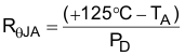
Knowing the maximum RθJA, the minimum amount of PCB copper area needed for appropriate heat sinking can be estimated using Figure 8-7.

GUID-3EC4CA58-E8CB-4F27-8D9E-4E6CC0383EA8-low.gif
RθJA value at board size of 9 in2 (that is, 3 inches × 3 inches) is a JEDEC standard.
Figure 8-7 RθJA versus Board Size

Figure 8-7 shows the variation of RθJA as a function of ground plane copper area in the board. Figure 8-7 is intended only as a guideline to demonstrate the affects of heat spreading in the ground plane; do not use Figure 8-7 to estimate actual thermal performance in real application environments.

Note:

When the device is mounted on an application PCB, TI strongly recommends using ΨJT and ΨJB, as explained in the Thermal Considerations section.