ZHCSN49M january   2007  – april 2023

PRODUCTION DATA  

  1. 特性
  2. 应用
  3. 描述
  4. Revision History
  5. Pin Configuration and Functions
  6. Specifications
    1. 6.1  Absolute Maximum Ratings
    2. 6.2  ESD Ratings
    3. 6.3  Recommended Operating Conditions
    4. 6.4  Thermal Information
    5. 6.5  Electrical Characteristics: Other Orderable Devices (non-M3 Suffix)
    6. 6.6  Electrical Characteristics: Orderable Device with M3 suffix
    7. 6.7  典型特性:IOUT = 50 mA
    8. 6.8  Typical Characteristics: IOUT = 1 A
    9. 6.9  Typical Characteristics: IOUT = 50 mA (M3 Suffix)
    10. 6.10 Typical Characteristics: IOUT = 1 A (M3 Suffix)
  7. Detailed Description
    1. 7.1 Overview
    2. 7.2 Functional Block Diagram
    3. 7.3 Feature Description
      1. 7.3.1 Enable/Shutdown
      2. 7.3.2 Power Good
      3. 7.3.3 Internal Current Limit
      4. 7.3.4 Thermal Protection
    4. 7.4 Device Functional Modes
      1. 7.4.1 Normal Operation
      2. 7.4.2 Dropout Operation
      3. 7.4.3 Disabled
    5. 7.5 Programming
      1. 7.5.1 Programmable Soft-Start
      2. 7.5.2 Sequencing Requirements
  8. Application and Implementation
    1. 8.1 Application Information
      1. 8.1.1 Adjusting the Output Voltage
      2. 8.1.2 Input, Output, and Bias Capacitor Requirements
      3. 8.1.3 Transient Response
      4. 8.1.4 Dropout Voltage
      5. 8.1.5 Output Noise
    2. 8.2 Typical Applications
      1. 8.2.1 FPGA I/O Supply at 1.5 V With a Bias Rail
        1. 8.2.1.1 Design Requirements
        2. 8.2.1.2 Detailed Design Procedure
        3. 8.2.1.3 Application Curves
      2. 8.2.2 FPGA I/O Supply at 1.5 V Without a Bias Rail
        1. 8.2.2.1 Design Requirements
        2. 8.2.2.2 Detailed Design Procedure
        3. 8.2.2.3 Application Curves
    3. 8.3 Power Supply Recommendations
    4. 8.4 Layout
      1. 8.4.1 Layout Guidelines
        1. 8.4.1.1 Estimating Junction Temperature
      2. 8.4.2 Layout Example
  9. Device and Documentation Support
    1. 9.1 Device Support
      1. 9.1.1 Development Support
        1. 9.1.1.1 Evaluation Modules
        2. 9.1.1.2 Spice Models
    2. 9.2 Documentation Support
      1. 9.2.1 Related Documentation
    3. 9.3 接收文档更新通知
    4. 9.4 支持资源
    5. 9.5 Trademarks
    6. 9.6 静电放电警告
    7. 9.7 术语表
  10. 10Mechanical, Packaging, and Orderable Information

封装选项

机械数据 (封装 | 引脚)
散热焊盘机械数据 (封装 | 引脚)
订购信息

Enable/Shutdown

The enable (EN) pin is active high and is compatible with standard digital signaling levels. VEN below 0.4 V turns the regulator off, while VEN above 1.1 V turns the regulator on. Unlike many regulators, the enable circuitry has hysteresis and deglitching for use with relatively slowly ramping analog signals. This configuration allows the TPS748 to be enabled by connecting the output of another supply to the EN pin. The enable circuitry typically has 50 mV of hysteresis and a deglitch circuit to help avoid on-off cycling as a result of small glitches in the VEN signal.

The enable threshold is typically 0.8 V and varies with temperature and process variations. Temperature variation is approximately –1 mV/°C; process variation accounts for most of the rest of the variation to the 0.4-V and 1.1-V limits. If precise turn-on timing is required, a fast rise-time signal must be used to enable the TPS748.

If not used, EN can be connected to either IN or BIAS. If EN is connected to IN, connect this pin as close as possible to the largest capacitance on the input to prevent voltage droops on that line from triggering the enable circuit.

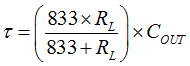
The TPS748 has an internal active pulldown circuit that connects the output to GND through an 833-Ω resistor when the device is disabled. This resistor discharges the output with a time constant of:

Equation 1. GUID-57CE021A-68AE-45B8-9F8C-669DA6663396-low.gif