ZHCSN49M january   2007  – april 2023

PRODUCTION DATA  

  1. 特性
  2. 应用
  3. 描述
  4. Revision History
  5. Pin Configuration and Functions
  6. Specifications
    1. 6.1  Absolute Maximum Ratings
    2. 6.2  ESD Ratings
    3. 6.3  Recommended Operating Conditions
    4. 6.4  Thermal Information
    5. 6.5  Electrical Characteristics: Other Orderable Devices (non-M3 Suffix)
    6. 6.6  Electrical Characteristics: Orderable Device with M3 suffix
    7. 6.7  典型特性:IOUT = 50 mA
    8. 6.8  Typical Characteristics: IOUT = 1 A
    9. 6.9  Typical Characteristics: IOUT = 50 mA (M3 Suffix)
    10. 6.10 Typical Characteristics: IOUT = 1 A (M3 Suffix)
  7. Detailed Description
    1. 7.1 Overview
    2. 7.2 Functional Block Diagram
    3. 7.3 Feature Description
      1. 7.3.1 Enable/Shutdown
      2. 7.3.2 Power Good
      3. 7.3.3 Internal Current Limit
      4. 7.3.4 Thermal Protection
    4. 7.4 Device Functional Modes
      1. 7.4.1 Normal Operation
      2. 7.4.2 Dropout Operation
      3. 7.4.3 Disabled
    5. 7.5 Programming
      1. 7.5.1 Programmable Soft-Start
      2. 7.5.2 Sequencing Requirements
  8. Application and Implementation
    1. 8.1 Application Information
      1. 8.1.1 Adjusting the Output Voltage
      2. 8.1.2 Input, Output, and Bias Capacitor Requirements
      3. 8.1.3 Transient Response
      4. 8.1.4 Dropout Voltage
      5. 8.1.5 Output Noise
    2. 8.2 Typical Applications
      1. 8.2.1 FPGA I/O Supply at 1.5 V With a Bias Rail
        1. 8.2.1.1 Design Requirements
        2. 8.2.1.2 Detailed Design Procedure
        3. 8.2.1.3 Application Curves
      2. 8.2.2 FPGA I/O Supply at 1.5 V Without a Bias Rail
        1. 8.2.2.1 Design Requirements
        2. 8.2.2.2 Detailed Design Procedure
        3. 8.2.2.3 Application Curves
    3. 8.3 Power Supply Recommendations
    4. 8.4 Layout
      1. 8.4.1 Layout Guidelines
        1. 8.4.1.1 Estimating Junction Temperature
      2. 8.4.2 Layout Example
  9. Device and Documentation Support
    1. 9.1 Device Support
      1. 9.1.1 Development Support
        1. 9.1.1.1 Evaluation Modules
        2. 9.1.1.2 Spice Models
    2. 9.2 Documentation Support
      1. 9.2.1 Related Documentation
    3. 9.3 接收文档更新通知
    4. 9.4 支持资源
    5. 9.5 Trademarks
    6. 9.6 静电放电警告
    7. 9.7 术语表
  10. 10Mechanical, Packaging, and Orderable Information

封装选项

机械数据 (封装 | 引脚)
散热焊盘机械数据 (封装 | 引脚)
订购信息

Estimating Junction Temperature

Using the thermal metrics ΨJT and ΨJB, as shown in the Thermal Information table, the junction temperature can be estimated with corresponding formulas (given in Equation 8). For backwards compatibility, an older θJC,Top parameter is listed as well.

Equation 8. GUID-DA650505-F492-4806-9E0F-5D59BED771A0-low.gif

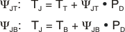
Where PD is the power dissipation shown by Equation 6, TT is the temperature at the center-top of the device package, and TB is the PCB temperature measured 1 mm away from the device package on the PCB surface (Figure 8-14).

Note: Both TT and TB can be measured on actual application boards using a thermo-gun (an infrared thermometer).

For more information about measuring TT and TB, see the Using New Thermal Metrics application note, available for download at www.ti.com.

GUID-38BC517E-DD8B-4D91-811A-47B95435EAC6-low.gifFigure 8-14 Measuring Points for TT and TB

By looking at Figure 8-15, the new thermal metrics (ΨJT and ΨJB) have very little dependency on board size. That is, using ΨJT or ΨJB with Equation 8 is a good way to estimate TJ by simply measuring TT or TB, regardless of the application board size.

GUID-82802605-9472-44B0-8A3E-8B2EC31D0A44-low.gifFigure 8-15 ΨJT and ΨJB vs Board Size

For a more detailed discussion of why TI does not recommend using θJC(top) to determine thermal characteristics, see the Using New Thermal Metrics application note, available for download at www.ti.com. For further information, see the IC Package Thermal Metrics application note, also available on the TI website.