ZHCSE51 September 2015 TPS657095
PRODUCTION DATA.
- 1 特性
- 2 应用
- 3 说明
- 4 修订历史记录
- 5 Pin Configuration and Functions
- 6 Specifications
-
7 Detailed Description
- 7.1 Overview
- 7.2 Functional Block Diagram
- 7.3
Feature Description
- 7.3.1 State Diagram
- 7.3.2 Power-up Timing
- 7.3.3 GPO
- 7.3.4 GPIO
- 7.3.5 LED_EN
- 7.3.6 Minimum-On-Time Feature
- 7.3.7 PWM Dimming
- 7.3.8 Crystal Oscillator and CLKOUT
- 7.3.9 LDOs
- 7.3.10 Undervoltage Lockout
- 7.3.11 Power Up/Power Down Default States
- 7.3.12 Output Voltage Discharge for LDO1 and LDO2
- 7.3.13 Power-Good Status Bits for LDO1 and LDO2
- 7.3.14 Short-Circuit Protection
- 7.3.15 Thermal Shutdown
- 7.3.16 LED Driver
- 7.3.17 4kByte OTP Memory
- 7.4 Device Functional Modes
- 7.5 Programming
- 7.6
Register Map
- 7.6.1 DEV_AND_REV_ID Register Address: 00h
- 7.6.2 OTP_REV Register Address: 01h
- 7.6.3 GPIO_CTRL Register Address: 02h
- 7.6.4 PWM_OSC_CNTRL Register Address: 03h
- 7.6.5 ISINK_CURRENT Register Address: 04h
- 7.6.6 LDO_CTRL Register Address: 05h
- 7.6.7 LDO1_VCTRL Register Address: 06h
- 7.6.8 LDO2_VCTRL Register Address: 07h
- 7.6.9 PWM_DUTY_THR_L Register Address: 08h
- 7.6.10 PWM_DUTY_THR_H Register Address: 09h
- 7.6.11 MIN_ON_TIME_THR Register Address: 0Ah
- 7.6.12 PWM_DUTY_L Register Address: 0Bh
- 7.6.13 PWM_DUTY_H Register Address: 0Ch
- 7.6.14 MIN_ON_TIME Register Address: 0Dh
- 7.6.15 SPARE Register Address: 0Eh
- 7.6.16 4K_OTP_PASSWORD Register Address: 0Fh
- 8 Application and Implementation
- 9 Power Supply Recommendations
- 10Layout
- 11器件和文档支持
- 12机械、封装和可订购信息
6 Specifications
6.1 Absolute Maximum Ratings
over operating free-air temperature range (unless otherwise noted)(1)| MIN | MAX | UNIT | ||
|---|---|---|---|---|
| Voltage | All pins except GND pin with respect to AGND | –0.3 | 7 | V |
| GPIO and GPO pull-up voltage if configured as open drain output | -0.3 | VCC + 0.3 | V | |
| Pin VLDO1 and VLDO2 with respect to AGND | –0.3 | 3.6 | V | |
| Current | VLDO1, VLDO2, VCC | 200 | mA | |
| GND, ISINK, GPIO, GPO | 50 | mA | ||
| All other pins | 3 | mA | ||
| Operating free-air temperature, TA | –40 | 85 | °C | |
| Maximum junction temperature, TJ | 125 | °C | ||
| Storage temperature range, Tstg | –65 | 150 | °C | |
(1) Stresses beyond those listed under absolute maximum ratings may cause permanent damage to the device. These are stress ratings only and functional operation of the device at these or any other conditions beyond those indicated under recommended operating conditions is not implied. Exposure to absolute-maximum-rated conditions for extended periods may affect device reliability.
6.2 ESD Ratings
| VALUE | UNIT | |||
|---|---|---|---|---|
| V(ESD) | Electrostatic discharge | Human body model (HBM), per ANSI/ESDA/JEDEC JS-001(1) | 2000 | V |
| Charged device model (CDM), per JEDEC specification JESD22-C101(2) | 500 | V | ||
(1) JEDEC document JEP155 states that 500-V HBM allows safe manufacturing with a standard ESD control process.
(2) JEDEC document JEP157 states that 250-V CDM allows safe manufacturing with a standard ESD control process.
6.3 Recommended Operating Conditions
over operating free-air temperature range (unless otherwise noted)| MIN | NOM | MAX | UNIT | ||
|---|---|---|---|---|---|
| VCC /AVCC | Input voltage range | 3.7 | 6 | V | |
| CVCC | Input capacitor at VCC | 1 | µF | ||
| CAVCC | Input capacitor at AVCC | 1 | µF | ||
| VLDOx | Output voltage range for LDO1 and LDO2 | 0.8 | 3.3 | V | |
| ILDO | Output current at LDO1 or LDO2 | 75 | mA | ||
| COUTLDO1/2 | Output capacitance at VLDO1, VLDO2 | 2.2 | 6.8 | µF | |
| LED_EN | Voltage range | 1.3 | 6 | V | |
| GPIO | Voltage range (configured as an input) | 1.3 | 3.3 | V | |
| TA | Operating ambient temperature | –40 | 85 | °C | |
| TJ | Operating junction temperature | –40 | 125 | °C | |
6.4 Thermal Information
| THERMAL METRIC(1) | TPS657095 | UNIT | |
|---|---|---|---|
| YFF (DSBGA) | |||
| 16 PINS | |||
| RθJA | Junction-to-ambient thermal resistance | 78.2 | °C/W |
| RθJC(top) | Junction-to-case (top) thermal resistance | 0.6 | |
| RθJB | Junction-to-board thermal resistance | 13.2 | |
| ψJT | Junction-to-top characterization parameter | 2.5 | |
| ψJB | Junction-to-board characterization parameter | 13 | |
| RθJC(bot) | Junction-to-case (bottom) thermal resistance | n/a | |
(1) For more information about traditional and new thermal metrics, see the IC Package Thermal Metrics application report, SPRA953.
6.5 Electrical Characteristics
Unless otherwise noted: VCC = AVCC = 5V, CVCC = 1µF; COUTLDOx= 2.2µF, TA = –40°C to 85°C| PARAMETER | TEST CONDITIONS | MIN | TYP | MAX | UNIT | |
|---|---|---|---|---|---|---|
| SUPPLY CURRENT | ||||||
| VCC, AVCC | Supply voltage | During normal operation | 3.7 | 6 | V | |
| During programming (writing) of OTP memory | -5% | 5 | +5% | V | ||
| IQ | Operating quiescent current | LDO1 disabled LDO2 disabled No I2C communications LED_EN = 0 CLKout_EN = 0 24MHz crystal disabled |
25 | 30 | μA | |
| LDO1 disabled LDO2 enabled, IOUT(LDO2) = 0 mA No I2C communications LED_EN = 0 CLKout_EN = 0 24MHz crystal disabled |
40 | 55 | uA | |||
| LDO1 enabled, IOUT(LDO1) = 0 mA LDO2 disabled No I2C communications LED_EN = 0 CLKout_EN = 0 24MHz crystal disabled |
40 | 55 | μA | |||
| LDO1 enabled, IOUT(LDO1) = 0 mA LDO2 enabled, IOUT(LDO2) = 0 mA No I2C communications LED_EN = 0 CLKout_EN = 0 24MHz crystal disabled |
60 | 80 | μA | |||
| LDO1 enabled, IOUT(LDO1) = 0 mA LDO2 enabled, IOUT(LDO2) = 0 mA No I2C communications LED_EN = 0 CLKout_EN = 1 24MHz crystal enabled |
2900 | 3550 | μA | |||
| LDO1 enabled, IOUT(LDO1) = 0 mA LDO2 enabled, IOUT(LDO2) = 0 mA No I2C communications LED_EN = 1, PWM Duty Cycle set to 99.9%, ISINK = 2mA CLKout_EN = 1 24MHz crystal enabled |
3000 | 3600 | μA | |||
| ISD | Shutdown current | Device disabled; VCC and AVCC < 1.8V |
45 | 85 | μA | |
| LED_ENABLE | ||||||
| VIH | High level input voltage | 1.1 | VCC | V | ||
| VIL | Low level input voltage | 0.4 | V | |||
| I(in)lkg | Input Leakage Current | 0.1 | μA | |||
| Input Deglitch | With a minimum pulse period of 500ns before another glitch is received | 100 | ns | |||
| GENERAL PURPOSE INPUT/OUTPUT (GPIO) | ||||||
| VIH | High level input voltage | For VLDO1 = 1.8V | 1.1 | VLDO1 | V | |
| VIH | High level input voltage | For VLDO1 = 3.3V | 1.37 | VLDO1 | V | |
| VIL | Low level input voltage | For VLDO1 = 1.8V | 0 | 0.4 | V | |
| VIL | Low level input voltage | For VLDO1 = 3.3V | 0 | 0.6 | V | |
| I(in)lkg | Input leakage current | GPIO programmed as input and tied to GND or VCC | 0.01 | 0.1 | μA | |
| VOH | High level output voltage | Configured as a push-pull output, IOH = 1mA, VLDO1 ≥ 1.8V | 1.2 | VLDO1-0.2V | VLDO1 | V |
| VOH | High level output voltage | Configured as a push-pull output, IOH = 1mA, 1.3V ≤ VLDO1 ≤1.8V | 1.0 | VLDO1 | V | |
| VOL | Low level output voltage | Configured as a push-pull output, IOL= 2mA, VLDO1 ≥ 1.8V | 0.25 | V | ||
| VOL | Low level output voltage | Configured as a push-pull output, IOL= 2mA, 1.3V ≤ VLDO1 ≤1.8V | 0.3 | V | ||
| VOL | Low level output voltage | Configured as an open-drain output, IOL= 4mA, VLDO1 ≥ 1.8V | 0.6 | V | ||
| VOL | Low level output voltage | Configured as an open-drain output, IOL= 2mA, 1.3V ≤ VLDO1 ≤1.8V | 0.6 | V | ||
| I(out)lkg | Output leakage current | Configured as an open-drain output, GPIO connected to VLDO1 | 0.01 | 0.1 | μA | |
| GENERAL PURPOSE OUTPUT (GPO) | ||||||
| VOH | High level output voltage | Configured as a push-pull output, IOH = 1mA, VLDO1 ≥ 1.8V | 1.2 | VLDO1-0.2V | VLDO1 | V |
| VOH | High level output voltage | Configured as a push-pull output, IOH = 1mA, 1.3V ≤ VLDO1 ≤ 1.8V | 1.0 | VLDO1 | V | |
| VOL | Low level output voltage | Configured as a push-pull output, IOL= 2mA, VLDO1 ≥ 1.8V | 0.25 | V | ||
| VOL | Low level output voltage | Configured as a push-pull output, IOL= 2mA, 1.3V ≤ VLDO1 ≤ 1.8V | 0.3 | V | ||
| VOL | Low level output voltage | Configured as an open-drain output, IOL= 4mA, VLDO1 ≥ 1.8V | 0.6 | V | ||
| VOL | Low level output voltage | Configured as an open-drain output, IOL= 2mA, 1.3V ≤ VLDO1 ≤1.8V | 0.6 | V | ||
| I(out)lkg | Output leakage current | Configured as an open-drain output, GPO connected to VLDO1 | 0.01 | 0.1 | μA | |
| SCL, SDA | ||||||
| VIH | High level input voltage on SCL, SDA | 1.2 | Vcc | V | ||
| VIL | Low level input voltage on SCL, SDA | 0 | 0.4 | V | ||
| Ilkg | Pin leakage current on SCL, SDA (includes leakage current for the open-drain output) | Input at VIL or VIH | 100 | nA | ||
| VOL | Low level output voltage on SDA | For IOL= 1mA | 0.25 | V | ||
| UNDERVOLTAGE LOCKOUT (UVLO), SENSED AT PIN AVCC | ||||||
| UVLO | Internal undervoltage lockout threshold | AVCC rising | 3.4 | 3.6 | 3.7 | V |
| Internal undervoltage lockout threshold hysteresis | AVCC falling | 130 | mV | |||
| CLOCK GENERATOR | ||||||
| fosc | Frequency of external crystal | 24 | MHz | |||
| fCLKOUT | Frequency on pin CLKOUT | For OSC_FREQ[1,0] = 00 | 24 | MHz | ||
| For OSC_FREQ[1,0] = 01 | 12 | |||||
| For OSC_FREQ[1,0] = 10 | 6 | |||||
| For OSC_FREQ[1,0] = 11 | 3 | |||||
| Period jitter; rms | Measured period compared to the Average Period of 10,000 randomly selected cylces | 600 | ps | |||
| Peak period to period jitter | Measured period compared to the Average Period of 10,000 randomly selected cylces | 600 | ps | |||
| Duty cycle of CLKout | 40% | 50% | 60% | |||
| Rise time / fall time for clock output | 10% to 90% of output voltage, 1.3V ≤ VLDO1 ≤ 3.3V | 10 | ns | |||
| Load capacitance | Defines the maximum capacitance that can be driven by the CLKOUT buffer and still meet the specified rise/fall times | 15 | pF | |||
| Output impedance | 50 | Ω | ||||
| VOH | High level output voltage | Internally connected to VLDO1≥ 1.8V: for COUT = 15pF, IOH = 1mA | 1.6 | VLDO1
- 0.2V |
VLDO1 | V |
| VOL | Low level output voltage | For COUT = 15pF, IOL = 1mA | 0.2 | 0.3 | V | |
| tstart | Oscillator start-up time | Time from CLKout_EN=1 to CLKout active for the NXTBD-24.000M crystal, not tested in production but based on simulations | 10 | ms | ||
| THERMAL PROTECTION | ||||||
| TSD | Thermal shutdown | Increasing junction temperature | 150 | °C | ||
| Thermal shutdown hysteresis | Decreasing junction temperature | 30 | °C | |||
| VLDO1, VLDO2 LOW DROPOUT REGULATORS | ||||||
| VCC | Input voltage range for LDO1 and LDO2 | 3.7 | 6 | V | ||
| VLDO1 | LDO1 output voltage | See LDO1_CTRL Register definition for all available voltage settings. | 0.8 | 1.8 | 3.3 | V |
| VLDO2 | LDO2 output voltage | See LDO2_CTRL Register definition for all available voltage settings. | 0.8 | 1.2 | 3.3 | V |
| IO | Output current for LDO1 and LDO2 | 100 | mA | |||
| ISC | LDO1 and LDO2 short circuit current limit | VLDOx = GND | 110 | 220 | mA | |
| Dropout voltage at LDO1 and LDO2 | IO = 75mA; VCC ≥ 3.7V | 700 | mV | |||
| Output voltage accuracy for LDO1 and LDO2 | VCC = VLDO + 0.6V (min 3.7V) to 6V, IO = 2mA through 75mA T = 0°C to 85°C |
–1.5% | 1.5% | |||
| Load Transient | VCC=AVCC=5V, IO(LDOx)= 0A to 75mA in 1us | 10% | ||||
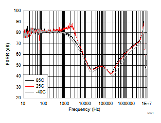
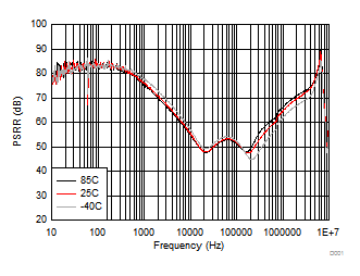
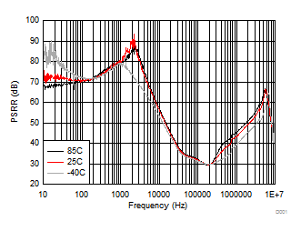
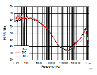
| PSRR | Power supply rejection ratio | f = 10kHz, COUT ≥ 2.2μF VINLDOx = 5V, VOUT = 1.8V, IOUT = 75mA, | 56 | dB | ||
| Output voltage rms noise | Voltage ripple and noise from 10kHz to 5MHz; Normal mode | 4 | mV | |||
| tRamp | VOUT ramp time |
Time to ramp from 5% to 95% of VOUT |
24 | 50 | 200 | µs |
| RDIS | Internal discharge resistor at VLDO1 and VLDO2 | VIN < UVLO | 200 | 400 | 550 | Ω |
| MINIMUM ON TIME | ||||||
| Minimum on time range | 0 | 11 | s | |||
| Minimum on time accuracy | Accuracy based on the Minimum On Time Setting (1 LSB = 44ms) | -1 | 1 | LSB | ||
| LED CURRENT SINK | ||||||
| ILED | Isink current (LED current for 99.9% duty cycle) |
|
10 | mA | ||
| Minimum voltage drop from ISINK to GND needed for proper regulation | At ISINK = 10mA | 0.3 | V | |||
| ISINK accuracy | ISINK = 10mA, Duty Cycle set to 99.9% | –10% | 5% | V | ||
| PWM frequency seetings | For PWM_FREQ[1,0] = 00 | 23.5 | kHz | |||
| For PWM_FREQ[1,0] = 01 | 11.7 | |||||
| For PWM_FREQ[1,0] = 10 | 5.8 | |||||
| For PWM_FREQ[1,0] = 11 | 2.9 | |||||
| PWM duty cycle range | Limited by ISINK rise / fall time for PWM_FREQ[1:0] other than 2'b11 setting | 0% | 99.9% | |||
| ISINK rise / fall time | V(ISINK) ≥ 0.6V for 2 mA ≤ ISINK ≤ 30mA | 400 | ns | |||
6.6 Timing Requirements
| MIN | MAX | UNIT | ||
|---|---|---|---|---|
| fMAX | Clock frequency | 400 | kHz | |
| t(HIGH) | Clock high time | 600 | ns | |
| t(LOW) | Clock low time | 1300 | ns | |
| tr | DATA and CLK rise time | 300 | ns | |
| tf | DATA and CLK fall time | 300 | ns | |
| thd;STA | Hold time (repeated) START condition (after this period the first clock pulse is generated) | 600 | ns | |
| tsu;STA | Setup time for repeated START condition | 600 | ns | |
| thd;DAT | Data input hold time | 10 | ns | |
| tsu;DAT | Data input setup time | 100 | ns | |
| tsu;STO | STOP condition setup time | 600 | ns | |
| tBUF | Bus free time | 1300 | ns | |
| Cl | load capacitance on SDA and SCL (with a 730 Ω or smaller pull-up resistor on SDA and SCL pulled up to 1.8V) | 400 | pF | |
 Figure 1. Serial I/f Timing Diagram
6.7 Typical Characteristics


