SLVSCA6C October 2013 – October 2017 TPS65311-Q1
PRODUCTION DATA.
- 1 Features
- 2 Applications
- 3 Description
- 4 Revision History
- 5 Description (continued)
- 6 Pin Configuration and Functions
- 7 Specifications
-
8 Detailed Description
- 8.1 Overview
- 8.2 Functional Block Diagram
- 8.3
Feature Description
- 8.3.1 Buck Controller (BUCK1)
- 8.3.2 Synchronous Buck Converters BUCK2 and BUCK3
- 8.3.3 BOOST Converter
- 8.3.4 Frequency-Hopping Spread Spectrum
- 8.3.5 Linear Regulator LDO
- 8.3.6 Gate Driver Supply
- 8.3.7 RESET
- 8.3.8 Soft Start
- 8.3.9 Power-on Reset Flag
- 8.3.10 WAKE Pin
- 8.3.11 IRQ Pin
- 8.3.12 VBAT Undervoltage Warning
- 8.3.13 VIN Over or Undervoltage Protection
- 8.3.14 External Protection
- 8.3.15 Overtemperature Detection and Shutdown
- 8.3.16 Independent Voltage Monitoring
- 8.3.17 GND Loss Detection
- 8.3.18 Reference Voltage
- 8.3.19 Shutdown Comparator
- 8.3.20 LED and High-Side Switch Control
- 8.3.21 Window Watchdog
- 8.3.22 Timeout in Start-Up Modes
- 8.4 Device Functional Modes
- 8.5 Programming
- 8.6 Register Map
-
9 Application and Implementation
- 9.1 Application Information
- 9.2
Typical Applications
- 9.2.1 Buck Controller (BUCK1)
- 9.2.2 Synchronous Buck Converters BUCK2 and BUCK3
- 9.2.3 BOOST Converter
- 9.2.4 Linear Regulator
- 10Power Supply Recommendations
- 11Layout
- 12Device and Documentation Support
- 13Mechanical, Packaging, and Orderable Information
7 Specifications
7.1 Absolute Maximum Ratings
over operating free-air temperature range (unless otherwise noted)(1)| MIN | MAX | UNIT | |||
|---|---|---|---|---|---|
| Supply inputs | VIN | –0.3 | 80 | V | |
| VINPROT | –0.3 | 60 | |||
| VSUP2, 3 (BUCK2 and 3) | –0.3 | 20 | |||
| VSUP4 (Linear Regulator) | –0.3 | 20 | |||
| VBOOST | –0.3 | 20 | |||
| EXTSUP | –0.3 | 13 | |||
| VIO | –0.3 | 5.5 | |||
| Buck controller | PH1 | –1 –2 for 100 ns |
60 | V | |
| VSENSE1 | –0.3 | 20 | |||
| COMP1 | –0.3 | 20 | |||
| GU-PH1, GL-PGND1, BOOT1-PH1 | –0.3 | 8 | |||
| S1, S2 | –0.3 | 20 | |||
| S1-S2 | –2 | 2 | |||
| BOOT1 | –0.3 | 68 | |||
| VMON1 | –0.3 | 20 | |||
| Buck controller | BOOT2, BOOT3 | –1 | 20 | V | |
| PH2, PH3 | –1(4)
–2 for 10 ns |
20(4) | |||
| VSENSE2, VSENSE3 | –0.3 | 20 | |||
| COMP2, COMP3 | –0.3 | 20 | |||
| VMON2, VMON3 | –0.3 | 20 | |||
| BOOTx – PHx | –0.3 | 8 | |||
| Linear regulator | LDO_OUT | –0.3 | 8 | V | |
| VSENSE4 | –0.3 | 20 | |||
| Boost converter | VSENSE5 | –0.3 | 20 | V | |
| PH5 | –0.3 | 20 | |||
| COMP5 | –0.3 | 20 | |||
| Digital interface | CSN, SCK, SDO, SDI, WD, HSPWM | –0.3 | 5.5 | V | |
| RESN, PRESN, IRQ | –0.3 | 20 | |||
| Wake input | WAKE | –1(3) | 60 | V | |
| Protection FET | GPFET | –0.3 | 80 | V | |
| VIN – GPFET | –0.3 | 20 | |||
| Battery sense input | VSSENSE | –1(3) | 60 Transients up to 80 V(2) |
V | |
| Temperature sense | VT | –0.3 | 5.5 | V | |
| VT_REF | –0.3 | 20 | |||
| Reference voltage | VREF | –0.3 | 5.5 | V | |
| High-side and LED driver | HSSENSE | –0.3 | 60 | V | |
| HSCTRL | –0.3 | 60 | |||
| VINPROT-HSSENSE, VINPROT-HSCTRL | –0.3 | 20 | |||
| Driver supply decoupling | VREG | –0.3 | 8 | V | |
| Supply decoupling | DVDD | –0.3 | 3.6 | V | |
| Temperature ratings | Junction temperature range, TJ | –55 | 150 | °C | |
| Operating temperature range, TA | –55 | 125 | |||
| Storage temperature, Tstg | –55 | 165 | |||
(1) Stresses beyond those listed under Absolute Maximum Ratings may cause permanent damage to the device. These are stress ratings only and functional operation of the device at these or any other conditions beyond those indicated under Recommended Operating Conditions is not implied. Exposure to absolute-maximum-rated conditions for extended periods may affect device reliability.
(2) Internally clamped to 60-V, 20-kΩ external resistor required, current into pin limited to 1 mA.
(3) Imax = 100 mA
(4) Maximum 3.5 A
7.2 ESD Ratings
| VALUE | UNIT | ||||
|---|---|---|---|---|---|
| V(ESD) | Electrostatic discharge | Human-body model (HBM), per AEC Q100-002(1) | ±1000 | V | |
| Charged-device model (CDM), per AEC Q100-011 | VT pin | ±150 | |||
| Corner pins (1, 14, 15, 28, 29, 42, 43, and 56) | ±750 | ||||
| All other pins | ±500 | ||||
(1) AEC Q100-002 indicates that HBM stressing shall be in accordance with the ANSI/ESDA/JEDEC JS-001 specification.
7.3 Recommended Operating Conditions
over operating free-air temperature range (unless otherwise noted)7.4 Thermal Information
| THERMAL METRIC(1) | TPS65311-Q1 | UNIT | ||
|---|---|---|---|---|
| RWE (VQFNP) | RVJ (VQFN) | |||
| 56 PINS | 56 PINS | |||
| RθJA | Junction-to-ambient thermal resistance | 22.1 | 22.3 | °C/W |
| RθJC(top) | Junction-to-case (top) thermal resistance | 9.6 | 9.8 | °C/W |
| RθJB | Junction-to-board thermal resistance | 6.2 | 6.3 | °C/W |
| ψJT | Junction-to-top characterization parameter | 0.1 | 0.1 | °C/W |
| ψJB | Junction-to-board characterization parameter | 6.2 | 6.2 | °C/W |
| RθJC(bot) | Junction-to-case (bottom) thermal resistance | 0.4 | 0.7 | °C/W |
(1) For more information about traditional and new thermal metrics, see the Semiconductor and IC Package Thermal Metrics application report.
7.5 Electrical Characteristics
VIN = VINPROT 4.8 V to 40 V, VSUPx = 3 V to 5.5 V, EXTSUP = 0 V, TJ(max) = 150°C, unless otherwise noted| PARAMETER | TEST CONDITIONS | MIN | TYP | MAX | UNIT | ||
|---|---|---|---|---|---|---|---|
| INPUT VOLTAGE-CURRENT CONSUMPTION | |||||||
| VIN | Device operating range | Buck regulator operating range, Voltage on VIN and VINPROT pins | 4 | 50 | V | ||
| VPOR | Power-on reset threshold | Falling VIN | 3.5 | 3.6 | 3.8 | V | |
| Rising VIN | 3.9 | 4.2 | 4.3 | ||||
| VPOR_hyst | Power-on reset hysteresis on VIN | 0.47 | 0.6 | 0.73 | V | ||
| ILPM0 | LPM0 current consumption(1)(3) | All off, wake active, VIN = 13 V Total current into VSSENSE, VIN and VINPROT |
44 | μA | |||
| ILPM0 | LPM0 current (commercial vehicle application) consumption(2)(3) | All off, wake active, VIN = 24.5 V Total current into VSSENSE, VIN and VINPROT |
60 | μA | |||
| IACTIVE1 | ACTIVE total current consumption(1)(4) | BUCK1 = on, VIN = 13 V, EXTSUP = 0 V, Qg of BUCK1 FETs = 15 nC. Total current into VSSENSE, VIN and VINPROT |
32 | mA | |||
| IACTIVE123 | ACTIVE total current consumption(1)(4) | BUCK1/2/3 = on, VIN = 13 V, Qg of BUCK1 FETs = 15 nC. Total current into VSSENSE, VIN and VINPROT |
40 | mA | |||
| IACTIVE1235 | ACTIVE current consumption(1)(4) | BUCK1/2/3, LDO, BOOST, high-side switch = on, VIN = 13 V, Qg of BUCK1 FETs = 15 nC. EXTSUP = 5 V from BOOST Total current into VSSENSE, VIN and VINPROT |
31 | mA | |||
| IACTIVE1235_noEXT | ACTIVE current consumption(1)(4) | BUCK1/2/3, LDO, BOOST, high-side switch = on, VIN = 13 V, Qg of BUCK1 FETs = 15 nC, EXTSUP = open Total current into VSENSE, VIN and VINPROT |
53 | mA | |||
| BUCK CONTROLLER (BUCK1) | |||||||
| VBUCK1 | Adjustable output voltage range | 3 | 11 | V | |||
| VSense1_NRM | Internal reference voltage in operating mode | VSENSE1 pin, load = 0 mA, Internal REF = 0.8 V |
–1% | 1% | |||
| VS1-2 | VS1-2 for forward OC in CCM | Maximum sense voltage VSENSE1 = 0.75 V (low duty cycle) | 60 | 75 | 90 | mV | |
| Minimum sense voltage VSENSE 1 = 1 V (negative current limit) | –65 | –37.5 | –23 | ||||
| ACS | Current sense voltage gain | ∆VCOMP1 / ∆ (VS1 - VS2) | 4 | 8 | 12 | V/V | |
| IGpeak | Gate driver peak current | VREG = 5.8 V | 0.6 | A | |||
| RDSON_DRIVER | Source and sink driver | IG current for external MOSFET = 200 mA, VREG = 5.8 V, VBOOT1-PH1 = 5.8 V |
5 | 10 | Ω | ||
| VDIO1 | Bootstrap diode forward voltage | IBOOT1 = –200 mA, VREG-BOOT1 | 0.8 | 1.1 | V | ||
| ERROR AMPLIFIER (OTA) FOR BUCK CONTROLLERS AND BOOST CONVERTER | |||||||
| gmEA | Forward transconductance | COMP1/2/3/5 = 0.8 V; source/sink = 5 µA, Test in feedback loop |
0.9 | mS | |||
| AEA | Error amplifier DC gain | 60 | dB | ||||
| SYNCHRONOUS BUCK CONVERTER BUCK2 AND BUCK3 (BUCK2/3) | |||||||
| VSUP2/3 | Supply voltage | 3 | 11 | V | |||
| VBUCK2/3 | Regulated output voltage range | Iload = 0…2 A VSUPx = VBUCK2/3 + Iload × 0.2 Ω |
0.8 | 5.5 | V | ||
| RDSON-HS | RDSON high-side switch | VBOOTx –PHx = 5.8 V | 0.20 | Ω | |||
| RDSON-LS | RDSON low-side switch | VREG = 5.8 V | 0.20 | Ω | |||
| IHS-Limit | High-side switch current-limit | Static current limit test. In application L > 1 µH at IHS-Limit and ILS-Limit to limit dI / dt |
2.5 | 2.9 | 3.3 | A | |
| ILS-Limit | Low-side switch current-limit | Static current limit test. In application L > 1 µH at IHS-Limit and ILS-Limit to limit dI / dt |
2 | 2.5 | 3 | A | |
| VSUPLkg | VSUP leakage current | VSUP = 10 V for high side, controller disabled, TJ = 100°C |
1 | 2 | µA | ||
| VSense2/3 | Feedback voltage | With respect to the 800-mV internal reference | –1% | 1% | |||
| COMP2/3HTH | COMP2/3 Input threshold low | 0.9 | 1.5 | V | |||
| COMP2/3LTH | COMP2/3 Input threshold high | VREG – 1.2 | VREG – 0.3 | V | |||
| RTIEOFF COMP23 | COMP2/3 internal tie-off | BUCK2/3 enabled. Resistor to VREG and GND, each | 70 | 100 | 130 | kΩ | |
| VDIO2 3 | Bootstrap diode forward voltage | IBOOT1 = –200 mA, VREG-BOOT2, VREG-BOOT3 | 1.1 | 1.2 | V | ||
| BOOST CONVERTER | |||||||
| VBoost | Boost adjustable output voltage range | Using 3.3-V input voltage, Ieak_switch ≤ 1 A | 4.5 | 15 | V | ||
| VBoost | Boost adjustable output voltage range | Using 3.3-V input voltage Iloadmax = 20 mA, Ipeak_switch = 0.3 A |
15 | 18.5 | V | ||
| RDS-ON_BOOST | Internal switch on-resistance | VREG = 5.8 V | 0.3 | 0.5 | Ω | ||
| VSense5 | Feedback voltage | With respect to the 800-mV internal reference | –1% | 1% | |||
| ICLBOOST | Internal switch current-limit | 1 | 1.5 | A | |||
| LINEAR REGULATOR LDO | |||||||
| VSUP4 | Device operating range for LDO | Recommended operating range | 3 | 7 | V | ||
| VLDO | Regulated output range | IOUT = 1 mA to 350 mA | 0.8 | 5.25 | V | ||
| VRefLDO | DC output voltage tolerance at VSENSE4 | VSENSE4 = 0.8 V (regulated at internal ref) VSUP4 = 3 V to 7 V, IOUT = 1 mA to 350 mA |
–2% | 2% | |||
| Vstep1 | Load step 1 | VSENSE4 = 0.8 V (regulated at internal ref) IOUT = 1 mA to 101 mA, CLDO = 6 to 50 µF, trise = 1 µs |
–2% | 2% | |||
| VSense4 | Feedback voltage | With respect to the 800-mV internal reference | –1% | 1% | |||
| VDropout | Drop out voltage | IOUT = 350 mA, TJ = 25°C | 127 | 143 | mV | ||
| IOUT = 350 mA, TJ = 125°C | 156 | 180 | |||||
| IOUT = 350 mA, TJ = 150°C | 275 | 335 | |||||
| IOUT | Output current | VOUT in regulation | –350 | –1 | mA | ||
| ILDO-CL | Output current limit | VOUT = 0 V, VSUP4 = 3 V to 7 V | –1000 | –400 | mA | ||
| PSRRLDO | Power supply ripple rejection | Vripple = 0.5 VPP, IOUT = 300 mA, CLDO = 10 µF |
Freq = 100 Hz | 60 | dB | ||
| Freq = 4 kHz | 50 | ||||||
| Freq = 150 kHz | 25 | ||||||
| LDOns10-100 | Output noise 10 Hz – 100 Hz | 10-µF output capacitance, VLDO = 2.5 V | 20 | µV/√(Hz) | |||
| LDOns100-1k | Output noise 100 Hz – 10 kHz | 10-µF output capacitance, VLDO = 2.5 V | 6 | µV/√(Hz) | |||
| CLDO | Output capacitor | Ceramic capacitor with ESR range, CLDO_ESR = 0 to 100 mΩ | 6 | 50 | µF | ||
| LED AND HIGH-SIDE SWITCH CONTROL | |||||||
| VHSSENSE | Current sense voltage | VINPROT – HSSENSE, high-side switch in current limit | 370 | 400 | 430 | mV | |
| VCMHSSENSE | Common mode range for current sensing | See VINPROT | 4 | 60 | V | ||
| VHSOL_TH | VINPROT – HSSENSE open load threshold | Ramping negative | 5 | 20 | 35 | mV | |
| Ramping positive | 26 | 38 | 50 | ||||
| VHSOL_HY | Open load hysteresis | 10 | 18 | 28 | mV | ||
| VHS SC | VINPROT – HSSENSE load short detection threshold | Ramping positive | 88% | 92.5% | 96% | VHSSENSE | |
| Ramping negative from load short condition | 87 | 90 | 93 | % of VHSSENSE | |||
| VHSSC_HY | VINPROT – HSSENSE short circuit hysteresis | 1 | % of VHSSENSE | ||||
| VHSCTRLOFF | Voltage at HSCTRL when OFF | VINPROT – 0.5 |
VINPROT | V | |||
| VGS | Clamp voltage between HSSENSE – HSCTRL | 6.1 | 7.7 | 8.5 | V | ||
| VOS_HS | Overshoot during turn-on | VOS_HS = VINPROT - HSSENSE | 400 | mV | |||
| ICL_HSCTRL | HSCTRL current-limit | 2 | 4.1 | 5 | mA | ||
| RPU_HSCTRL | Internal pullup resistors | Between VINPROT and HSCTRL | 70 | 100 | 130 | kΩ | |
| RPU_HSCTRL-HSSENSE | Between HSCTRL and HSSENSE | 70 | 100 | 130 | |||
| VI_high | High level input voltage | HSPWM, VIO = 3.3 V | 2 | V | |||
| VI_low | Low level input voltage | HSPWM, VIO = 3.3 V | 0.8 | V | |||
| VI_hys | Input voltage hysteresis | HSPWM, VIO = 3.3 V | 150 | 500 | mV | ||
| RSENSE | External sense resistor | Design info, no device parameter | 1.5 | 50 | Ω | ||
| CGS | External MOSFET gate source capacitance | 100 | 2000 | pF | |||
| CGD | External MOSFET gate drain capacitance | 500 | pF | ||||
| REFERENCE VOLTAGE | |||||||
| VREF | Reference voltage | 3.3 | V | ||||
| VREF-tol | Reference voltage tolerance | IVREF = 5 mA | –1% | 1% | |||
| IREFCL | Reference voltage current-limit | 10 | 25 | mA | |||
| CVREF | Capacitive load | 0.6 | 5 | µF | |||
| REFns10-100 | Output noise 10 Hz–100 Hz | 2.2 µF output capacitance, IVREF = 5 mA | 20 | µV/√(Hz) | |||
| REFns100-1k | Output noise 100 Hz–10 kHz | 2.2 µF output capacitance, IVREF = 5 mA | 6 | µV/√(Hz) | |||
| VREF_OK | Reference voltage OK threshold | Threshold, VREF falling | 2.91 | 3.07 | 3.12 | V | |
| Hysteresis | 14 | 70 | 140 | mV | |||
| SHUTDOWN COMPARATOR | |||||||
| VT_REF | Shutdown comparator reference voltage | IVT_REF = 20 µA. Measured as drop voltage with respect to VDVDD | 10 | 17 | 500 | mV | |
| IVT_REF = 600 µA. Measured as drop voltage with respect to VDVDD. No VT_REF short-circuit detection. | 200 | 420 | 1100 | ||||
| IVT_REFCL | Shutdown comparator reference current limit | VT_REF = 0 | 0.6 | 1 | 1.4 | mA | |
| VVT_REF SH | VT_REF short circuit detection | Threshold, VT_REF falling. Measured as drop voltage with respect to VDVDD | 0.9 | 1.2 | 1.8 | V | |
| Hysteresis | 130 | mV | |||||
| VTTH-H | Input voltage threshold on VT, rising edge triggers shutdown | This feature is specified by design to work down to –55°C. | 0.48 | 0.50 | 0.52 | VT_REF | |
| VTTH-L | Input voltage threshold on VT, falling voltage enables device operation | This feature is specified by design to work down to –55°C. | 0.46 | 0.48 | 0.52 | VT_REF | |
| VTTOL | Threshold variation | VTTH-H – VT_REF / 2, VTTH-L – VT_REF / 2 | –20 | 20 | mV | ||
| IVT_leak | Leakage current | TJ: –20°C to 125°C | –400 | –50 | nA | ||
| TJ: –55°C to –20°C | –200 | –50 | |||||
| VT_REFOV | VT_REF overvoltage threshold | Threshold, VT_REF rising. Measured as drop voltage with respect to VDVDD | 0.42 | 0.9 | 1.2 | V | |
| Hysteresis | 100 | mV | |||||
| WAKE INPUT | |||||||
| VWAKE_ON | Voltage threshold to enable device | WAKE pin is a level sensitive input | 3.3 | 3.7 | V | ||
| VBAT UNDERVOLTAGE WARNING | |||||||
| VSSENSETH_L | VSSENSE falling threshold low | SPI selectable, default after reset | 4.3 | 4.7 | V | ||
| VSSENSETH_H | VSSENSE falling threshold high | SPI selectable | 6.2 | 6.8 | V | ||
| VSSENSE-HY | VSSENSE hysteresis | 0.2 | V | ||||
| IVSLEAK | Leakage current at VSSENSE | LPM0 mode, VSSENSE 55 V | 1 | µA | |||
| IVSLEAK60 | Leakage current at VSSENSE | LPM0 mode, VSSENSE 60 V | 100 | µA | |||
| IVSLEAK80 | Leakage current at VSSENSE | LPM0 mode, VSSENSE 80 V | 5 | 25 | mA | ||
| RVSSENSE | Internal resistance from VSSENSE to GND | VSSENSE = 14 V, disabled in LPM0 mode | 0.7 | 1 | 1.3 | MΩ | |
| VIN OVERVOLTAGE PROTECTION | |||||||
| VOVTH_H | VIN overvoltage shutdown threshold 1 (rising edge) | Selectable with SPI | 50 | 60 | V | ||
| VOVTH_L | VIN overvoltage shutdown threshold 2 (rising edge) | Selectable with SPI, default after reset | 36 | 38 | V | ||
| VOVHY | VIN overvoltage hysteresis | Threshold 1 | 0.2 | 1.7 | 3 | V | |
| Threshold 2 - default after reset | 1.5 | 2 | 2.5 | ||||
| WINDOW WATCHDOG | |||||||
| VI_high | High level input voltage | WD, VIO = 3.3 V | 2 | V | |||
| VI_low | Low level input voltage | WD, VIO = 3.3 V | 0.8 | V | |||
| VI_hys | Input voltage hysteresis | WD, VIO = 3.3 V | 150 | 500 | mV | ||
| RESET AND IRQ BLOCK | |||||||
| VRESL | Low level output voltage at RESN, PRESN and IRQ | VIN ≥ 3 V, IxRESN = 2.5 mA | 0 | 0.4 | V | ||
| VRESL | Low level output voltage at RESN and PRESN | VIN = 0 V, VIO = 1.2 V, IxRESN = 1 mA | 0 | 0.4 | V | ||
| IRESLeak | Leakage current at RESN, PRESN and IRQ | Vtest = 5.5 V | 1 | µA | |||
| NRES | Number of consecutive reset events for transfer to LPM0 | 7 | |||||
| EXTERNAL PROTECTION | |||||||
| VCLAMP | Gate to source clamp voltage | VIN - GPFET, 100 µA | 14 | 20 | V | ||
| IGPFET | Gate turn on current | VIN = 14 V, GPFET = 2 V | 15 | 25 | µA | ||
| RDSONGFET | Gate driver strength | VIN = 14 V, turn off | 25 | Ω | |||
| THERMAL SHUTDOWN AND OVERTEMPERATURE PROTECTION | |||||||
| TSDTH | Thermal shutdown | Junction temperature | 160 | 175 | °C | ||
| TSDHY | Hysteresis | 20 | °C | ||||
| TOTTH | Overtemperature flag | Overtemperature flag is implemented as local temp sensors and expected to trigger before the thermal shutdown | 150 | 165 | °C | ||
| TOTHY | Hysteresis | 20 | °C | ||||
| VOLTAGE MONITORS BUCK1/2/3, VIO, LDO, BOOSTER | |||||||
| VMONTH_L | Voltage monitor reference | REF = 0.8 V – falling edge | 90% | 92% | 94% | ||
| VMONTH_H | Voltage monitor reference | REF = 0.8 V – rising edge | 106% | 108% | 110% | ||
| VMON_HY | Voltage monitor hysteresis | 2% | |||||
| VVIOMON_TH | Undervoltage monitoring at VIO – falling edge | 3 | 3.13 | V | |||
| VVIOMON_HY | UV_VIO hysteresis | 0.05 | V | ||||
| GND LOSS | |||||||
| VGLTH-low | GND loss threshold low | GND to PGNDx | –0.31 | –0.25 | –0.19 | V | |
| VGLTH-high | GND loss threshold high | GND to PGNDx | 0.19 | 0.25 | 0.31 | V | |
| INTERNAL VOLTAGE REGULATORS | |||||||
| VREG | Internal regulated supply | IVREG = 0 mA to 50 mA, VINPROT = 6.3 V to 40 V and EXTSUP = 6.3 V to 12 V | 5.5 | 5.8 | 6.1 | V | |
| VEXTSUP-TH | Switch over voltage | IVREG = 0 mA to 50 mA and EXTSUP ramping positive, ACTIVE mode | 4.4 | 4.6 | 4.8 | V | |
| VEXTSUP-HY | Switch over hysteresis | 100 | 200 | 300 | mV | ||
| VREGDROP | Drop out voltage on VREG | IVREG = 50 mA, EXTSUP = 5 V / VINPROT = 5 V and EXTSUP = 0 V / VINPROT = 4 V |
200 | mV | |||
| IREG_CL | Current limit on VREG | EXTSUP = 0 V, VREG = 0 V | –250 | –50 | mA | ||
| IREG_EXTSUP_CL | EXTSUP ≥ 4.8 V, VREG = 0 V | –250 | –50 | mA | |||
| CVREG | Capacitive load | 1.2 | 2.2 | 3.3 | µF | ||
| VREG-OK | VREG undervoltage threshold | VREG rising | 3.8 | 4 | 4.2 | V | |
| Hysteresis | 350 | 420 | 490 | mV | |||
| VDVDD | Internal regulated low voltage supply | 3.15 | 3.3 | 3.45 | V | ||
| VDVDD UV | DVDD undervoltage threshold | DVDD falling | 2.1 | V | |||
| VDVDD OV | DVDD overvoltage threshold | DVDD rising | 3.8 | V | |||
| SPI | |||||||
| VI_high | High level input voltage | CSN, SCK, SDI; VIO = 3.3 V | 2 | V | |||
| VI_low | Low level input voltage | CSN, SCK, SDI; VIO = 3.3 V | 0.8 | V | |||
| VI_hys | Input voltage hysteresis | CSN, SCK, SDI; VIO = 3.3 V | 150 | 500 | mV | ||
| VO_high | SDO output high voltage | VIO = 3.3 V ISDO = 1 mA | 3 | V | |||
| VO_low | SDO output low voltage | VIO = 3.3 V ISDO = 1 mA | 0.2 | V | |||
| CSDO | SDO capacitance | 50 | pF | ||||
| GLOBAL PARAMETERS | |||||||
| RPU | Internal pullup resistor at CSN pin | 70 | 100 | 130 | kΩ | ||
| RPD | Internal pulldown resistor at pins: HSPWM , SDI, SCK, WD, S2(5) | 70 | 100 | 130 | kΩ | ||
| RPD-WAKE | Internal pulldown resistor at WAKE pin | 140 | 200 | 260 | kΩ | ||
| ILKG | Input pullup current at pins: - VSENSE1–5 - VMON1–3 |
VTEST = 0.8 V | –200 | –100 | –50 | nA | |
(1) TA = 25°C
(2) TA = 130°C
(3) Quiescent Current Specification does not include the current flow through the external feedback resistor divider. Quiescent Current is non-switching current, measured with no load on the output with VBAT = 13 V.
(4) Total current consumption measured on EVM includes switching losses.
(5) RAMP and ACTIVE only
7.6 Timing Requirements
| MIN | TYP | MAX | UNIT | |||
|---|---|---|---|---|---|---|
| BUCK CONTROLLER (BUCK1) | ||||||
| tOCBUCK1_BLK | RSTN and ERROR mode transition, when over current detected for > tOCBUCK1_BLK | 1 | ms | |||
| LED AND HIGH-SIDE SWITCH CONTROL | ||||||
| tHSOL_BLK | Open load blanking time | 70 | 100 | 140 | µs | |
| tHSS CL | Net time in current limit to disable driver | 4 | 5 | 6 | ms | |
| tS HS | Current-limit sampling interval | 100 | µs | |||
| tON | Turnon time | Time from rising HSPWM till high-side switch in current limitation, ±5% settling | 30 | µs | ||
| Time from rising HSPWM till high-side switch till voltage-clamp between HSSENSE – HSCTRL active (within VGS limits) | 30 | 60 | µs | |||
| fHS_IN | HSPWM input frequency | Design information, no device parameter | 100 | 500 | Hz | |
| REFERENCE VOLTAGE | ||||||
| TREF_OK | Reference voltage OK deglitch time | 10 | 20 | µs | ||
| SHUTDOWN COMPARATOR | ||||||
| TVT_REF_FLT | VT_REF fault deglitch time | Overvoltage or short condition on VT_REF | 10 | 20 | µs | |
| WAKE INPUT | ||||||
| tWAKE | Min. pulse width at WAKE to enable device | VWAKE = 4 V to suppress short spikes at WAKE pin | 10 | 20 | µs | |
| VBAT UNDERVOLTAGE WARNING | ||||||
| tVSSENSE_BLK | Blanking time | VVSENSE < VSSENSETH_xx → IRQ asserted | 10 | 35 | µs | |
| VIN OVERVOLTAGE PROTECTION | ||||||
| tOFF BLK-H | OV delay time | VIN > VOVTH_H → GPFET off | 1 | µs | ||
| tOFF BLK-L | OV blanking time | VIN > VOVTH_L → GPFET off | 10 | 20 | µs | |
| WINDOW WATCHDOG | ||||||
| ttimeout | Timeout | TESTSTART, TESTSTOP, VTCHECK , and RAMP mode: Starts after entering each mode. ACTIVE mode: WD timeout starts with rising edge of RESN |
230 | 300 | 370 | ms |
| tWD | Watchdog window time | Spread spectrum disabled | 18 | 20 | 22 | ms |
| Spread spectrum enable | 19.8 | 22 | 24.2 | |||
| tWD_FAIL | Closed window time | tWD / 4 | ||||
| tWD_BLK | WD filter time | 1.2 | µs | |||
| RESET AND IRQ BLOCK | ||||||
| tRESNHOLD | RESN hold time | 1.8 | 2 | 2.2 | ms | |
| tIRQHOLD | IRQ hold time | After VVSENSE < VSSENSETH for tVSSENSE_BLK | 10 | 20 | µs | |
| tDR IRQ PRESN | Rising edge delay of IRQ to rising edge of PRESN | 2 | µs | |||
| tDF RESN_PRESN | Falling edge delay of RESN to PRESN / IRQ | 2 | µs | |||
| THERMAL SHUTDOWN AND OVERTEMPERATURE PROTECTION | ||||||
| tSD-BLK | Blanking time before thermal shutdown | 10 | 20 | µs | ||
| tOT_BLK | Blanking time before thermal over temperature | 10 | 20 | µs | ||
| VOLTAGE MONITORS BUCK1/2/3, VIO, LDO, BOOSTER | ||||||
| tVMON_BLK | Blanking time between UV/OV condition to RESN low | UV/OV: BUCK1/2/3 UV: VIO | 10 | 20 | µs | |
| tVMONTHL_BLK | Blanking time between undervoltage condition to ERROR mode transition or corresponding SPI bit | BUCK1/2/3 → ERROR mode LDO or BOOST → SPI bit set or turn off | 1 | ms | ||
| tVMONTHL_BLK1 | Blanking time between undervoltage condition to ERROR mode transition | VIO only | 10 | 20 | µs | |
| tVMONTHH_BLK1 | Blanking time between overvoltage condition to ERROR mode transition | BUCK1/2/3 → ERROR mode VIO has no OV protection | 10 | 20 | µs | |
| tVMONTHH_BLK2 | Blanking time LDO and BOOST overvoltage condition to corresponding SPI bit or ERROR mode | LDO or BOOST (ACTIVE mode) → SPI bit set or turn off LDO (VTCHECK or RAMP mode) → ERROR mode | 20 | 40 | µs | |
| GND LOSS | ||||||
| tGL-BLK | Blanking time between GND loss condition and transition to ERROR state | 5 | 20 | µs | ||
| POWER-UP SEQUENCING | ||||||
| tSTART1 | Soft start time of BOOST | From start till exceeding VMONTH_L + VMON_HY Level | 0.7 | 2.7 | ms | |
| tSTART2 | Soft start time of BUCK1/2/3 and LDO | From start till exceeding VMONTH_L + VMON_HY Level | 0.5 | 2 | ms | |
| tSTART | Startup DVDD regulator | From start till exceeding VMONTH_L + VMON_HY Level | 3 | ms | ||
| tSEQ2 | Sequencing time from start of BUCK1 to BUCK2 and BOOST | Internal SSDONE_BUCK1 signal | 3 | ms | ||
| tWAKE-RES | Startup time from entering TESTSTART to RESN high | GPFET = IRFR6215 | 14 | ms | ||
| tSEQ1 | Sequencing time from start of BOOST to BUCK3 | Internal SSDONE_BOOST signal | 1 | 4 | ms | |
| INTERNAL VOLTAGE REGULATORS | ||||||
| tDVDD OV | Blanking time from DVDD overvoltage condition to shutdown mode transition | 10 | 20 | µs | ||
| SPI INTERFACE | ||||||
| tSPI | SCK period | See Figure 1 | 240 | ns | ||
| tSCKL | SCK low time | 100 | ns | |||
| tSCKH | SCK high time | 100 | ns | |||
| tFSIV | Time between falling edge of CSN and SDO output valid (FSI bit) | Falling SDO < 0.8 V; Rising SDO > 2 V, See Figure 1 | 80 | ns | ||
| tSDOV | Time between rising edge of SCK and SDO data valid | Falling SDO < 0.8 V; Rising SDO > 2 V, See Figure 1 | 55 | ns | ||
| tSDIS | Setup time of SDI before falling edge of SCK | See Figure 1 | 20 | ns | ||
| tSDOH | Hold time of SDO after rising edge of SCK | 5 | ns | |||
| tHCS | Hold time of CSN after last falling edge of SCK | See Figure 1 | 50 | ns | ||
| tSDOtri | Delay between rising edge of CSN and SDO 3-state | 80 | ns | |||
| tmin2SPI | Minimum time between two SPI commands | 10 | µs | |||
7.7 Switching Characteristics
over operating free-air temperature range (unless otherwise noted)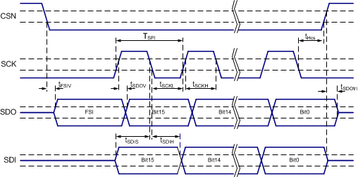 Figure 1. SPI Timing
7.8 Typical Characteristics
All parameters are measured on a TI EVM, unless otherwise specified.
7.8.1 BUCK 1 Characteristics
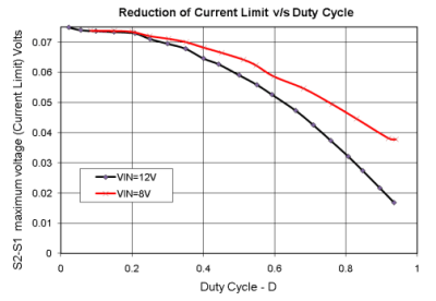
7.8.2 BUCK 2 and BUCK3 Characteristics
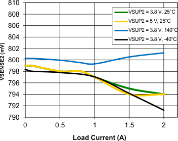
EXTSUP Pin Open
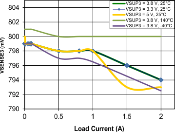
EXTSUP Pin Open
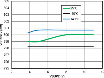
EXTSUP Pin Open
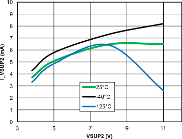
EXTSUP Pin Open
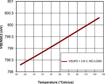
EXTSUP Pin Open
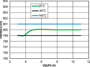
EXTSUP Pin Open
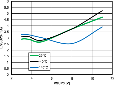
EXTSUP Pin Open
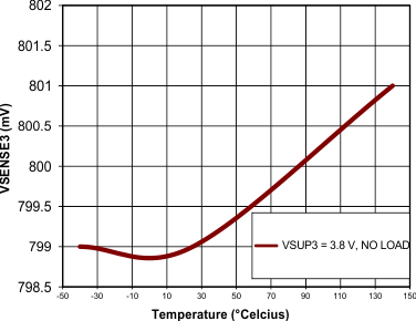
EXTSUP Pin Open
7.8.3 BOOST Characteristics
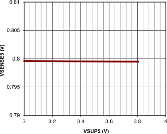 Figure 11. Open-Load Line Regulation BOOST = 5 V, AT 25°C, EXTSUP Pin Open, BOOST Supply Input = 3.8 V
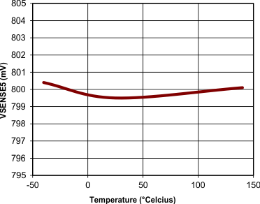 Figure 13. BOOST = 5-V VSENSE5 vs Temperature
EXTSUP Pin Open, Input Supply = 3.8-V, 0.4-A Load
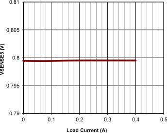 Figure 12. Load Regulation BOOST = 5 V AT 25°C
EXTSUP Pin Open, BOOST Supply Input = 3.8 V
7.8.4 LDO Noise Characteristics
(2 × 3.3-µF output capacitance, LDO output = 2.5 V, VSUP4 = 3.8 V)
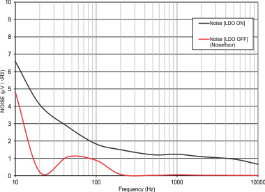 Figure 14. LDO Noise Density