SLVSCA6C October 2013 – October 2017 TPS65311-Q1
PRODUCTION DATA.
- 1 Features
- 2 Applications
- 3 Description
- 4 Revision History
- 5 Description (continued)
- 6 Pin Configuration and Functions
- 7 Specifications
-
8 Detailed Description
- 8.1 Overview
- 8.2 Functional Block Diagram
- 8.3
Feature Description
- 8.3.1 Buck Controller (BUCK1)
- 8.3.2 Synchronous Buck Converters BUCK2 and BUCK3
- 8.3.3 BOOST Converter
- 8.3.4 Frequency-Hopping Spread Spectrum
- 8.3.5 Linear Regulator LDO
- 8.3.6 Gate Driver Supply
- 8.3.7 RESET
- 8.3.8 Soft Start
- 8.3.9 Power-on Reset Flag
- 8.3.10 WAKE Pin
- 8.3.11 IRQ Pin
- 8.3.12 VBAT Undervoltage Warning
- 8.3.13 VIN Over or Undervoltage Protection
- 8.3.14 External Protection
- 8.3.15 Overtemperature Detection and Shutdown
- 8.3.16 Independent Voltage Monitoring
- 8.3.17 GND Loss Detection
- 8.3.18 Reference Voltage
- 8.3.19 Shutdown Comparator
- 8.3.20 LED and High-Side Switch Control
- 8.3.21 Window Watchdog
- 8.3.22 Timeout in Start-Up Modes
- 8.4 Device Functional Modes
- 8.5 Programming
- 8.6 Register Map
-
9 Application and Implementation
- 9.1 Application Information
- 9.2
Typical Applications
- 9.2.1 Buck Controller (BUCK1)
- 9.2.2 Synchronous Buck Converters BUCK2 and BUCK3
- 9.2.3 BOOST Converter
- 9.2.4 Linear Regulator
- 10Power Supply Recommendations
- 11Layout
- 12Device and Documentation Support
- 13Mechanical, Packaging, and Orderable Information
11 Layout
11.1 Layout Guidelines
11.1.1 Buck Controller
- Connect a local decoupling capacitor between the drain of Q3 and the source of Q2. The length of this trace loop should be short.
- The Kelvin-current sensing for the shunt resistor should have traces with minimum spacing, routed in parallel with each other. Place any filtering capacitor for noise near the S1-S2 pins.
- The resistor divider for sensing the output voltage connects between the positive pin of the output capacitor and the GND pin (IC signal ground). Do not locate these components and their traces near any switching nodes or high-current traces. The resistor divider for monitoring the output voltage is to be placed as close as possible to the sensing resistor divider, and should be connected to same traces.
- Connect the boot-strap capacitance between the PH1 and BOOT1 pins, and keep the length of these trace loops as short as possible.
- Connect the compensation network between the COMP1 pin and GND pin (IC signal ground).
- Connect a local decoupling capacitor between the VREG and PGDN1 pin, and between the EXTSUP and PGND1 pin. The length of this trace loop should be short.
11.1.2 Buck Converter
- Connect a local decoupling capacitor between VSUP2 and PGND2 respectively VSUP3 and PGND3 pins. The length of this trace loop should be short.
- The resistor divider for sensing the output voltage connects between the positive pin of the output capacitor and the GND pin (IC signal ground). Do not locate these components and their traces near any switching nodes or high-current traces. The resistor divider for monitoring the output voltage is to be placed as close as possible to the sensing resistor divider, and should be connected to same traces.
- Connect the boot-strap capacitance between the PH2 and BOOT2 respectively PH3 and BOOT3 pins, and keep the length of this trace loop as short as possible.
- If COMP2 and/or COMP3 are chosen to be connected to ground, use the signal ground trace connected to GND pin for this.
11.1.3 Boost Converter
- The path formed from the input capacitor to the inductor and the PH5 pin should have short trace length. The same applies for the trace from the inductor to Schottky diode D2 to the output capacitor and the VBOOST pin. Connect the negative pin of the input capacitor and the PGND5 pin together with short trace lengths.
- The resistor divider for sensing the output voltage connects between the positive pin of the output capacitor and the GND pin (IC signal ground). Do not locate these components and their traces near any switching nodes or high-current traces.
- Connect the compensation network between the COMP5 pin and GND pin (IC signal ground).
11.1.4 Linear Regulator
- Connect a local decoupling capacitor between VSUP4 and GND (IC signal ground) pins. The length of this trace loop should be short.
- The resistor divider for sensing the output voltage connects between the positive pin of the output capacitor and the GND pin (IC signal ground). Do not locate these components and their traces near any switching nodes or high-current traces.
11.1.5 Other Considerations
- Short PGNDx and GND to the thermal pad.
- Use a star ground configuration if connecting to a non-ground plane system. Use tie-ins for the compensation-network ground, voltage-sense feedback ground, and local biasing bypass capacitor ground networks to this star ground.
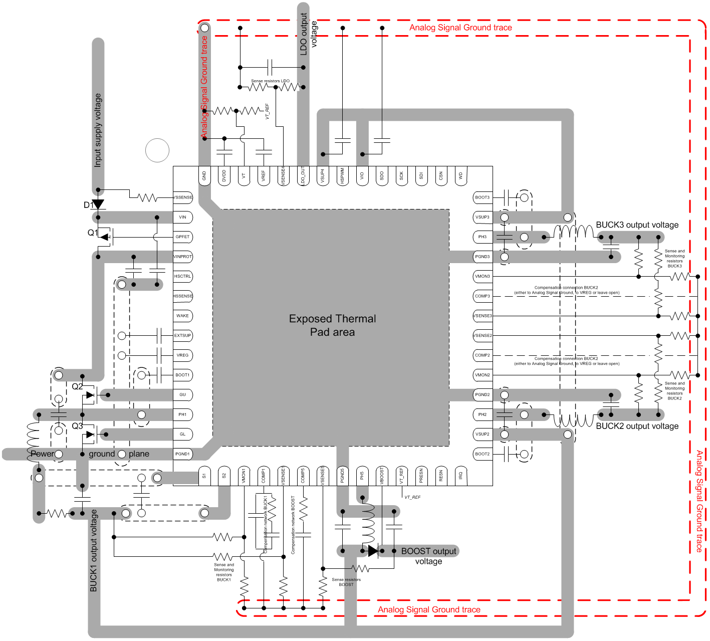
11.2 Layout Example
 Figure 41. TPS65311-Q1 Layout Example