SLVSCA6C October 2013 – October 2017 TPS65311-Q1
PRODUCTION DATA.
- 1 Features
- 2 Applications
- 3 Description
- 4 Revision History
- 5 Description (continued)
- 6 Pin Configuration and Functions
- 7 Specifications
-
8 Detailed Description
- 8.1 Overview
- 8.2 Functional Block Diagram
- 8.3
Feature Description
- 8.3.1 Buck Controller (BUCK1)
- 8.3.2 Synchronous Buck Converters BUCK2 and BUCK3
- 8.3.3 BOOST Converter
- 8.3.4 Frequency-Hopping Spread Spectrum
- 8.3.5 Linear Regulator LDO
- 8.3.6 Gate Driver Supply
- 8.3.7 RESET
- 8.3.8 Soft Start
- 8.3.9 Power-on Reset Flag
- 8.3.10 WAKE Pin
- 8.3.11 IRQ Pin
- 8.3.12 VBAT Undervoltage Warning
- 8.3.13 VIN Over or Undervoltage Protection
- 8.3.14 External Protection
- 8.3.15 Overtemperature Detection and Shutdown
- 8.3.16 Independent Voltage Monitoring
- 8.3.17 GND Loss Detection
- 8.3.18 Reference Voltage
- 8.3.19 Shutdown Comparator
- 8.3.20 LED and High-Side Switch Control
- 8.3.21 Window Watchdog
- 8.3.22 Timeout in Start-Up Modes
- 8.4 Device Functional Modes
- 8.5 Programming
- 8.6 Register Map
-
9 Application and Implementation
- 9.1 Application Information
- 9.2
Typical Applications
- 9.2.1 Buck Controller (BUCK1)
- 9.2.2 Synchronous Buck Converters BUCK2 and BUCK3
- 9.2.3 BOOST Converter
- 9.2.4 Linear Regulator
- 10Power Supply Recommendations
- 11Layout
- 12Device and Documentation Support
- 13Mechanical, Packaging, and Orderable Information
9 Application and Implementation
NOTE
Information in the following applications sections is not part of the TI component specification, and TI does not warrant its accuracy or completeness. TI’s customers are responsible for determining suitability of components for their purposes. Customers should validate and test their design implementation to confirm system functionality.
9.1 Application Information
The TPS65311-Q1 device is a multi-rail power supply including one buck controller, two buck converters, one boost converter and one linear regulator (LDO). The buck controller is typically used to convert a higher car battery voltage to a lower DC voltage which is then used as pre-regulated input supply for the buck converters, boost converter, and the linear regulator. Use the following design procedure and application example to select component values for the TPS65311-Q1 device.
9.2 Typical Applications
9.2.1 Buck Controller (BUCK1)
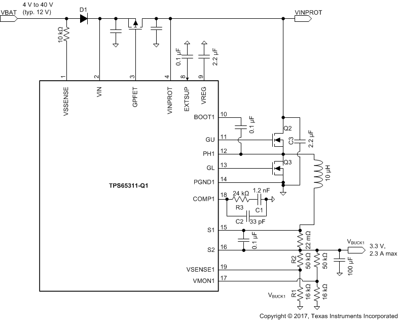 Figure 26. Buck Controller Schematic
9.2.1.1 Design Requirements
For this design example, use the parameters listed in Table 2.
Table 2. Design Parameters
| DESIGN PARAMETER | EXAMPLE VALUE |
|---|---|
| Input voltage | 12 V |
| Output voltage (VBUCK1) | 3.3 V |
| Maximum output current (Imax_peak_coil) | 2.3 A |
| Load Step ΔIOUT | 1 A |
| Output current ripple IL_ripple | 500 mA |
| Output voltage ripple | 3 mV |
| Allowed voltage step on output ΔVOUT | 0.198 (or 6%) |
| Switching frequency (fSWBUCK1) | 490 kHz |
| Bandwidth (FBW) | ≈ 60 kHz |
9.2.1.2 Detailed Design Procedure
9.2.1.2.1 Adjusting the Output Voltage for the BUCK1 Controller
A resistor divider from the output node to the VSENSE1 pin sets the output voltage. TI recommends using 1% tolerance or better divider resistors. Start with 16 kΩ for the R1 resistor and use Equation 1 to calculate R2 (see Figure 26).

Therefore, for the value of VBUCK1 to equal to 3.3 V, the value of R2 must be 50 kΩ.
For voltage monitoring of the BUCK1 output voltage, placing an additional resistive divider with the exact same values from the output node to the VMON1 pin is recommended for safety reasons (see Figure 26). If no safety standard must be fulfilled in the application, the VMON1 pin can be directly connected to VSENSE1 pin without the need for this additional resistive divider.
9.2.1.2.2 Output Inductor, Sense Resistor, and Capacitor Selection for the BUCK1 Controller
An external resistor senses the current through the inductor. The current sense resistor pins (S1 and S2) are fed into an internal differential amplifier which supports the range of VBUCK1 voltages. The sense resistor RS must be chosen so that the maximum forward peak current in the inductor generates a voltage of 75 mV across the sense pins. This specified typical value is for low duty cycles only. At typical duty-cycle conditions around 28% (assuming 3.3-V output and 12-V input), 50 mV is a more reasonable value, considering tolerances and mismatches. The typical characteristics (see Figure 2) provide a guide for using the correct current-limit sense voltage.

Optimal slope compensation which is adaptive to changes in input voltage and duty cycle allows stable operation at all conditions. In order to specify optimal performance of this circuit, the following condition must be satisfied in the choice of inductor and sense resistor:

where
- L = inductor in µH
- Rs = sense resistor in Ω
The current sense pins S1 and S2 are high impedance pins with low leakage across the entire VBUCK1 range. This allows DCR current sensing (see Figure 16) using the DC resistance of the inductor for better efficiency.
For selecting the output capacitance and its ESR resistance, the following set of equations can be used:
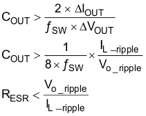
where
- ƒsw is the 490-kHz switching frequency
- ΔIOUT is the worst-case load step from the application
- ΔVOUT is the allowed voltage step on the output
- Vo_ripple is the allowed output voltage ripple
- IL_ripple is the ripple current in the coil
9.2.1.2.3 Compensation of the Buck Controller
The main buck controller requires external type 2 compensation on pin COMP1 for normal mode operation. The components can be calculated as follows.
- Select a value for the bandwidth, FBW, to be between fSWBUCK1 / 6 (faster response) and fSWBUCK1 / 10 (more conservative)
- Use Equation 5 to select a value for R3 (see Figure 16).
- COUT1 is the load capacitance of BUCK1
- gm is the error amplifier transconductance
- KCFB = 0.125 / Rs
- VrefBUCK is the internal reference voltage
- Use Equation 6 to select a value for C1 (in series with R3, see Figure 16) to set the zero frequency close to FBW / 10.
- Use Equation 7 to select a value for C2 (parallel with R3, C1, see Figure 16) to set the second pole below fSWBUCK1 / 2

where


For example:
fSWBUCK1 = 490 kHz, VrefBUCK = 0.8 V, FBW = 60 kHz
VOUT1 = 3.3 V, COUT1 = 100 µF, Rs = 22 mΩ
Selected values: R3 = 24 kΩ, C1 = 1.2 nF, C2 = 33 pF
Resulting in FBW: 58 kHz
Resulting in zero frequency: 5.5 kHz
Resulting in second pole frequency: 201 kHz
Stability and load step response must be verified in measurements to fine tune the values of the compensation components.
9.2.1.2.4 Bootstrap Capacitor for the BUCK1 Controller
The BUCK1 controller requires a bootstrap capacitor. This bootstrap capacitor must be 0.1 μF. The bootstrap capacitor is located between the PH1 pin and the BOOT1 pin (see Figure 26). The bootstrap capacitor must be a high-quality ceramic type with X7R or X5R grade dielectric for temperature stability.
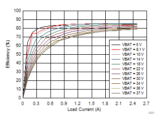
9.2.1.3 BUCK 1 Application Curve
9.2.2 Synchronous Buck Converters BUCK2 and BUCK3
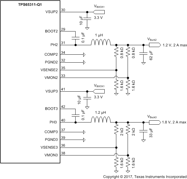 Figure 28. Synchronous Buck Converter Schematic
9.2.2.1 Design Requirements
For this design example, use the parameters listed in Table 3.
Table 3. Design Parameters
| DESIGN PARAMETER | EXAMPLE VALUE |
|---|---|
| Input voltage | 3.3 V |
| Output voltage (VBUCK2/3) | 1.2 V 1.8 V |
| Maximum output current (Imax_peak) | 2 A |
| Output current ripple ΔIL_PP | 300 mA |
| Switching frequency (fSWBUCK2/3) | 2.45 MHz |
9.2.2.2 Detailed Design Procedure
9.2.2.2.1 Adjusting the Output Voltage for the BUCK2 and BUCK3 Converter
A resistor divider from the output node to the VSENSE2 to ground respectively between the VSENSE3 to ground pin sets the output voltage (see Figure 28). TI recommends using 1% tolerance or better divider resistors. Start by selecting 1.6 kΩ for the value of the Rx resistor between the VSENSE2 to ground respectively between the VSENSE3 to ground pin VSENSE3 pin and use Equation 8 to calculate the value for the Ry resistor between BUCK2 and BUCK3 output and the VSENSE2 to ground respectively between the VSENSE3 to ground pin.

Therefore, for VBUCK2 to equal to 1.2 V, the value of Ry must be 0.8 kΩ. For VBUCK3 to equal to 1.8 V, the value of Ry must be 2 kΩ.
For voltage monitoring of the BUCK2 and BUCK3 output voltage, placing an additional resistive divider with exact same values from the output node to the VMON2 and VMON3 pins is recommended for safety reasons (see Figure 28). If no safety standard must be fulfilled in the application, the VMON2 and VMON3 pins can be directly connected to VSENSE2 and VSENSE3 pins without the need for this additional resistive divider.
9.2.2.2.2 Output Inductor Selection for the BUCK2 and BUCK3 Converter
The inductor value L depends on the allowed ripple current ΔIL_PP in the coil at chosen input voltage VIN and output voltage VOUT, and given switching frequency fsw:

For example:
VIN = 3.3 V (from BUCK1)
VOUT = 1.2 V
ΔIL_PP = 300 mA
fsw = 2.45 MHz
→ L ≈ 1 μH
9.2.2.2.3 Compensation of the BUCK2 and BUCK3 Converters
The regulators operate in forced continuous mode, and have internal frequency compensation. The frequency response can be adjusted to the selected LC filter by setting the COMP2 and COMP3 pin low, high, or floating. After selecting the output inductor value as previously described, the output capacitor must be chosen so that the L × COUT × VBUCK2/3 product is equal to or less than one of the three values, as listed in Table 4.
Table 4. Compensation Settings
| COMP 2/3 | L × COUT × VBUCK2/3 | EXAMPLE COMPONENTS |
|---|---|---|
| = 0 V | 80 µF × µH × V | 30 µF × 2.2 µH × 1.2 V |
| = OPEN | 160 µF × µH × V | 50 µF × 1.8 µH × 1.8 V |
| = VREG | 320 µF × µH × V | 150 µF × 2.2 µH × 1.2 V |
Larger output capacitors can be used if a feed-forward capacitor is placed across the upper resistance, Ry, of the feedback divider. This works effectively for output voltages > 2 V. With an RC product greater than 10 µs, the effective VBUCK2/3 at higher frequencies can be assumed as 0.8 V, thus allowing an output capacitor increase by a factor equal to the ratio of the output voltage to 0.8 V.
9.2.2.2.4 Bootstrap Capacitor for the BUCK2/3 Converters
The BUCK2 and BUCK3 converters require a bootstrap capacitor. This bootstrap capacitor must be 0.1 μF. The bootstrap capacitor is located between the PH2 pin and the BOOT2 pin and between the PH3 pin and the BOOT3 pin (see Figure 28). The bootstrap capacitor must be a high-quality ceramic type with X7R or X5R grade dielectric for temperature stability.
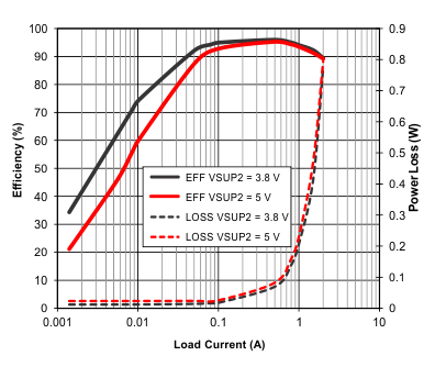
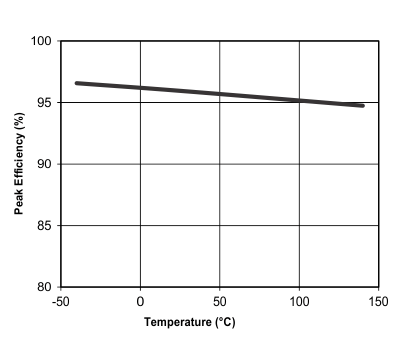
9.2.2.3 BUCK2 and BUCK3 Application Curves
| Buck2 = 3.3 V at 25°C | L = 1 μH | C = 20 μF |
| COMP2 Pin to Ground | EXTSUP Pin Open | |
| L = 1 μH | C = 20 μF | VSUP2 = 3.8 V |
| COMP2 Pin to Ground | EXTSUP Pin Open | |
| 0.5-A LOAD | ||
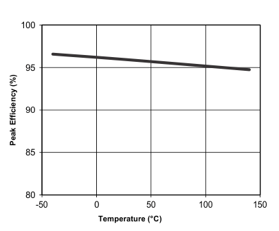
| L = 1 μH | C = 20 μF | VSUP2 = 3.8 V |
| COMP2 Pin to Ground | EXTSUP Pin Open | |
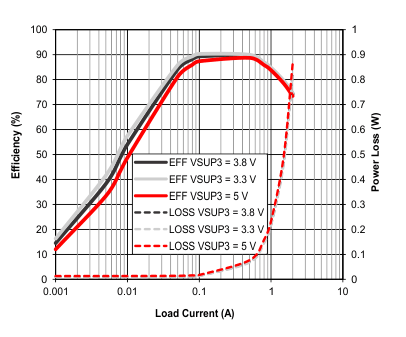
| Buck3 = 1.2 V at 25°C | L = 1.2 μH | C = 30 μF |
| EXTSUP Pin Open | COMP3 Pin to Ground | |
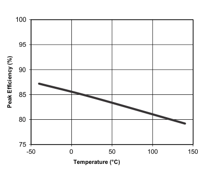
| L = 1.2 μH | C = 30 μF | VSUP3 = 3.8 V |
| EXTSUP Pin Open | 1-A LOAD | |
| COMP3 Pin to Ground | ||
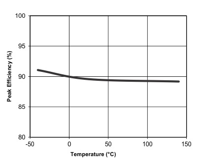
| L = 1.2 μH | C = 30 μF | VSUP3 = 3.8 V |
| EXTSUP Pin Open | COMP3 Pin to Ground | |
9.2.3 BOOST Converter
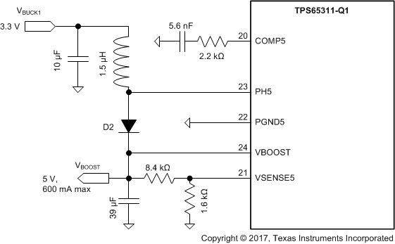 Figure 35. BOOST Converter Schematic
9.2.3.1 Design Requirements
For this design example, use the parameters listed in Table 5.
Table 5. Design Parameters
| DESIGN PARAMETER | EXAMPLE VALUE |
|---|---|
| Input voltage | 3.3 V |
| Output voltage (VBOOST) | 5 V |
| Peak coil current (Ipeak_coil) | 1 A |
| Maximum output current IOUT | ≈ 600 mA |
| Output current ripple ΔIL_PP | 300 mA |
| Switching frequency (fSWBOOST) | 2.45 MHz |
9.2.3.2 Detailed Design Procedure
9.2.3.2.1 Adjusting the Output Voltage for the Boost Converter
A resistor divider from the output node to the VSENSE5 pin sets the output voltage. TI recommends using 1% tolerance or better divider resistors. Start with a value of 1.6 kΩ for the Rx resistor and use Equation 10 to calculate Ry (see Figure 35).

Therefore, for the value of VBOOST to equal to 5 V, the value of Ry must be 8.4 kΩ.
9.2.3.2.2 Output Inductor and Capacitor Selection for the BOOST Converter
The inductor value L depends on the allowed ripple current ΔIL_PP in the coil at chosen input voltage VIN and output voltage VOUT, and given switching frequency fsw:

For example:
VIN = 3.3 V (from BUCK1)
VOUT = 5 V
ΔIL_PP = 300 mA (30% of 1-A peak current)
ƒsw = 2.45 MHz
→ L ≈ 1.5 μH
The capacitor value COUT must be selected such that the L-C double-pole frequency FLC is in the range of
10 kHz–15 kHz. The FLC is given by Equation 12:

The right half-plane zero FRHPZ, as given in Equation 13, must be > 200 kHz:

where
- IOUT represents the load current
If the condition FRHPZ > 200 kHz is not satisfied, L and therefore COUT have to be recalculated.
9.2.3.2.3 Compensation of the BOOST Converter
The BOOST converter requires an external R-C network for compensation (see Figure 15, COMP5). The components can be calculated using Equation 14 and Equation 15:


where
- FBW represents the bandwidth of the regulation loop, and must be set to 30 kHz
- FLC represents the L-C double-pole frequency, as mentioned previously
For example:
VIN = 3.3 V (from BUCK1)
VOUT = 5 V
L = 1.5 μH
C = 39 μF
→ FLC = 13.7 kHz
FBW = 30 kHz
→ R ≈ 2.2 kΩ
→ C ≈ 5.6 nF
Stability and load step response must be verified in measurements to fine tune the values of the compensation components.
9.2.3.2.4 Output Diode for the BOOST Converter
The BOOST converter requires an external output diode between the PH5 pin and VBOOST pin (see Figure 35, component D2). The selected diode must have a reverse voltage rating equal to or greater than the VBOOST output voltage. The peak current rating of the diode must be greater than the maximum inductor current. The diode must also have a low forward voltage in order to reduce the power losses. Therefore, Schottky diodes are typically a good choice for the catch diode.
Also, select a diode with an appropriate power rating, because the diode conducts the output current during the off-time of the internal power switch.
9.2.3.3 BOOST Converter Application Curves
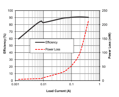
| BOOST Supply Input = 3.8 V | EXTSUP Pin Open | |
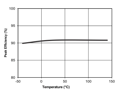
| BOOST Supply Input = 3.8 V | EXTSUP Pin Open | |
9.2.4 Linear Regulator
9.2.4.1 Design Requirements
For this design example, use the parameters listed in Table 6.
Table 6. Design Parameters
| DESIGN PARAMETER | EXAMPLE VALUE |
|---|---|
| Input voltage | 3.3 V |
| Output voltage (VLDO_OUT) | 2.5 V |
| Maximum output current (IOUT) | 350 mA |
9.2.4.2 Detailed Design Procedure
9.2.4.2.1 Adjusting the Output Voltage for the Linear Regulator
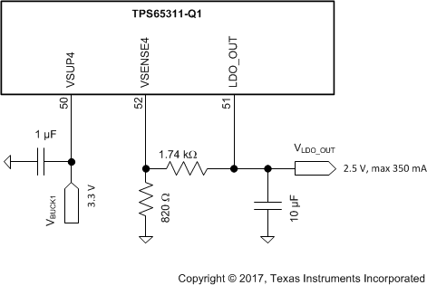
A resistor divider from the output node to the VSENSE4 pin sets the output voltage. TI recommends using 1% tolerance or better divider resistors. In order to get the minimum required load current of 1 mA for the linear regulator, start with a value of 820 Ω for the Rx resistor and use Equation 16 to calculate Ry (see Figure 38).

Therefore, for the value of VLDO_OUT to equal to 2.5 V, the value of Ry must be 1.74 kΩ.
9.2.4.2.2 Output Capacitance for the Linear Regulator
The linear regulator requires and external output capacitance with a value between 6 µF and 50 µF.
9.2.4.3 Linear Regulator Application Curve
