ZHCSDM4D december 2014 – may 2023 TPS65263-Q1
PRODUCTION DATA
- 1
- 1 特性
- 2 应用
- 3 说明
- 4 Revision History
- 5 Pin Configuration and Functions
- 6 Specifications
-
7 Detailed Description
- 7.1 Overview
- 7.2 Functional Block Diagram
- 7.3
Feature Description
- 7.3.1 Adjusting the Output Voltage
- 7.3.2 Enable and Adjusting UVLO
- 7.3.3 Soft-Start Time
- 7.3.4 Power-Up Sequencing
- 7.3.5 V7V Low-Dropout Regulator and Bootstrap
- 7.3.6 Out-of-Phase Operation
- 7.3.7 Output Overvoltage Protection (OVP)
- 7.3.8 PSM
- 7.3.9 Slope Compensation
- 7.3.10 Overcurrent Protection
- 7.3.11 Power Good
- 7.3.12 Thermal Shutdown
- 7.4 Device Functional Modes
- 7.5 Register Maps
- 8 Application and Implementation
- 9 Device and Documentation Support
- 10Mechanical, Packaging, and Orderable Information
7.3.1 Adjusting the Output Voltage
The output voltage of each buck is set with a resistor divider from the output of buck to the FB pin. TI recommends to use 1% tolerance or better resistors.
 Figure 7-1 Voltage Divider Circuit
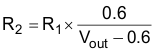
To improve efficiency at light loads consider using larger value resistors. If the values are too high, the regulator is more sensitive to noise. Table 7-1 shows the recommended resistor values.
| OUTPUT VOLTAGE (V) | R1 (kΩ) | R2 (kΩ) |
|---|---|---|
| 1 | 10 | 15 |
| 1.2 | 10 | 10 |
| 1.5 | 15 | 10 |
| 1.8 | 20 | 10 |
| 2.5 | 31.6 | 10 |
| 3.3 | 45.3 | 10 |
| 3.3 | 22.6 | 4.99 |
| 5 | 73.2 | 10 |
| 5 | 36.5 | 4.99 |
The output voltage of the buck converter can be dynamically scaled by I2C-controlled 7-bit register, VOUTx_SEL. Before I2C communication, the output voltage is set with the resistor divider from the output of buck to the FB pin. When the GO bit is set to 1 through the I2C interface, the buck converter switches the external resistor divider to the internal resistor divider as shown in Figure 7-2. The output voltage can be selected among 128 voltages with voltage identifications (VID) shown in Table 7-2. The output voltage range of dynamic voltage scaling is 0.68 to 1.95 V with 10-mV resolution of each voltage step.
 Figure 7-2 Voltage
Divider Circuit
Figure 7-2 Voltage
Divider Circuit| OUT_SEL <7:0> | VOUT (V) | VOUT_SEL <7:0> | VOUT (V) | VOUT_SEL <7:0> | VOUT (V) | VOUT_SEL <7:0> | VOUT (V) |
|---|---|---|---|---|---|---|---|
| 0 | 0.68 | 20 | 1 | 40 | 1.32 | 60 | 1.64 |
| 1 | 0.69 | 21 | 1.01 | 41 | 1.33 | 61 | 1.65 |
| 2 | 0.7 | 22 | 1.02 | 42 | 1.34 | 62 | 1.66 |
| 3 | 0.71 | 23 | 1.03 | 43 | 1.35 | 63 | 1.67 |
| 4 | 0.72 | 24 | 1.04 | 44 | 1.36 | 64 | 1.68 |
| 5 | 0.73 | 25 | 1.05 | 45 | 1.37 | 65 | 1.69 |
| 6 | 0.74 | 26 | 1.06 | 46 | 1.38 | 66 | 1.7 |
| 7 | 0.75 | 27 | 1.07 | 47 | 1.39 | 67 | 1.71 |
| 8 | 0.76 | 28 | 1.08 | 48 | 1.4 | 68 | 1.72 |
| 9 | 0.77 | 29 | 1.09 | 49 | 1.41 | 69 | 1.73 |
| A | 0.78 | 2A | 1.1 | 4A | 1.42 | 6A | 1.74 |
| B | 0.79 | 2B | 1.11 | 4B | 1.43 | 6B | 1.75 |
| C | 0.8 | 2C | 1.12 | 4C | 1.44 | 6C | 1.76 |
| D | 0.81 | 2D | 1.13 | 4D | 1.45 | 6D | 1.77 |
| E | 0.82 | 2E | 1.14 | 4E | 1.46 | 6E | 1.78 |
| F | 0.83 | 2F | 1.15 | 4F | 1.47 | 6F | 1.79 |
| 10 | 0.84 | 30 | 1.16 | 50 | 1.48 | 70 | 1.8 |
| 11 | 0.85 | 31 | 1.17 | 51 | 1.49 | 71 | 1.81 |
| 12 | 0.86 | 32 | 1.18 | 52 | 1.5 | 72 | 1.82 |
| 13 | 0.87 | 33 | 1.19 | 53 | 1.51 | 73 | 1.83 |
| 14 | 0.88 | 34 | 1.2 | 54 | 1.52 | 74 | 1.84 |
| 15 | 0.89 | 35 | 1.21 | 55 | 1.53 | 75 | 1.85 |
| 16 | 0.9 | 36 | 1.22 | 56 | 1.54 | 76 | 1.86 |
| 17 | 0.91 | 37 | 1.23 | 57 | 1.55 | 77 | 1.87 |
| 18 | 0.92 | 38 | 1.24 | 58 | 1.56 | 78 | 1.88 |
| 19 | 0.93 | 39 | 1.25 | 59 | 1.57 | 79 | 1.89 |
| 1A | 0.94 | 3A | 1.26 | 5A | 1.58 | 7A | 1.9 |
| 1B | 0.95 | 3B | 1.27 | 5B | 1.59 | 7B | 1.91 |
| 1C | 0.96 | 3C | 1.28 | 5C | 1.6 | 7C | 1.92 |
| 1D | 0.97 | 3D | 1.29 | 5D | 1.61 | 7D | 1.93 |
| 1E | 0.98 | 3E | 1.3 | 5E | 1.62 | 7E | 1.94 |
| 1F | 0.99 | 3F | 1.31 | 5F | 1.63 | 7F | 1.95 |