ZHCSP59B October 2021 – June 2022 TPS631000
PRODUCTION DATA
- 1 特性
- 2 应用
- 3 说明
- 4 Revision History
- 5 Pin Configuration and Functions
- 6 Specifications
- 7 Detailed Description
- 8 Application and Implementation
- 9 Power Supply Recommendations
- 10Layout
- 11Device and Documentation Support
- 12Mechanical, Packaging, and Orderable Information
8.2.2.5 Setting the Output Voltage
The output voltage is set by an external resistor divider. The resistor divider must be connected between VOUT, FB, and GND. The feedback voltage is 500 mV nominal.
The low-side resistor R2 (between FB and GND) should not exceed 100 kΩ. The high-side resistor (between FB and VOUT) R1 is calculated with Equation 4.
Equation 4. 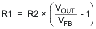
where
- VFB = 500 mV
Table 8-5 Resistor Selection For Typical Output Voltages
| VOUT | R1 | R2 |
|---|---|---|
| 2.5 V | 365 | 91 |
| 3.3 V | 511 | 91 |
| 3.6 V | 562 | 91 |
| 5 V | 806 | 91 |