ZHCSIN0K August 2018 – July 2025 TPS62810-Q1 , TPS62811-Q1 , TPS62812-Q1 , TPS62813-Q1
PRODUCTION DATA
9.2.2 详细设计过程
方程式 10. 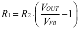
VFB = 0.6V 时:
表 9-2 设置输出电压
| 标称输出电压 VOUT | R1 | R2 | CFF | 确切输出电压 |
|---|---|---|---|---|
| 0.8V | 16.9kΩ | 51kΩ | 10pF | 0.7988V |
| 1.0V | 20kΩ | 30kΩ | 10pF | 1.0V |
| 1.1V | 39.2kΩ | 47kΩ | 10pF | 1.101V |
| 1.2V | 68kΩ | 68kΩ | 10pF | 1.2V |
| 1.5V | 76.8kΩ | 51kΩ | 10pF | 1.5V |
| 1.8V | 80.6kΩ | 40.2kΩ | 10pF | 1.803V |
| 2.5V | 47.5kΩ | 15kΩ | 10pF | 2.5V |
| 3.3V | 88.7kΩ | 19.6kΩ | 10pF | 3.315V |