ZHCSIN0J august   2018  – march 2023 TPS62810-Q1 , TPS62811-Q1 , TPS62812-Q1 , TPS62813-Q1

PRODUCTION DATA  

  1. 特性
  2. 应用
  3. 说明
  4. Revision History
  5. Device Comparison Table
  6. Pin Configuration and Functions
  7. Specifications
    1. 7.1 Absolute Maximum Ratings
    2. 7.2 ESD Ratings
    3. 7.3 Recommended Operating Conditions
    4. 7.4 Thermal Information
    5. 7.5 Electrical Characteristics
    6. 7.6 Typical Characteristics
  8. Parameter Measurement Information
    1. 8.1 Schematic
  9. Detailed Description
    1. 9.1 Overview
    2. 9.2 Functional Block Diagram
    3. 9.3 Feature Description
      1. 9.3.1 Precise Enable
      2. 9.3.2 COMP/FSET
      3. 9.3.3 MODE / SYNC
      4. 9.3.4 Spread Spectrum Clocking (SSC)
      5. 9.3.5 Undervoltage Lockout (UVLO)
      6. 9.3.6 Power Good Output (PG)
      7. 9.3.7 Thermal Shutdown
    4. 9.4 Device Functional Modes
      1. 9.4.1 Pulse Width Modulation (PWM) Operation
      2. 9.4.2 Power Save Mode Operation (PWM/PFM)
      3. 9.4.3 100% Duty-Cycle Operation
      4. 9.4.4 Current Limit and Short Circuit Protection
      5. 9.4.5 Foldback Current Limit and Short Circuit Protection
      6. 9.4.6 Output Discharge
      7. 9.4.7 Soft Start / Tracking (SS/TR)
  10. 10Application and Implementation
    1. 10.1 Application Information
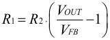
      1. 10.1.1 Programming the Output Voltage
      2. 10.1.2 External Component Selection
        1. 10.1.2.1 Inductor Selection
      3. 10.1.3 Capacitor Selection
        1. 10.1.3.1 Input Capacitor
        2. 10.1.3.2 Output Capacitor
    2. 10.2 Typical Application
      1. 10.2.1 Design Requirements
      2. 10.2.2 Detailed Design Procedure
      3. 10.2.3 Application Curves
    3. 10.3 System Examples
      1. 10.3.1 Fixed Output Voltage Versions
      2. 10.3.2 Voltage Tracking
      3. 10.3.3 Synchronizing to an External Clock
    4. 10.4 Power Supply Recommendations
    5. 10.5 Layout
      1. 10.5.1 Layout Guidelines
      2. 10.5.2 Layout Example
  11. 11Device and Documentation Support
    1. 11.1 Device Support
      1. 11.1.1 第三方产品免责声明
    2. 11.2 Documentation Support
      1. 11.2.1 Related Documentation
    3. 11.3 接收文档更新通知
    4. 11.4 支持资源
    5. 11.5 Trademarks
    6. 11.6 静电放电警告
    7. 11.7 术语表
  12. 12Mechanical, Packaging, and Orderable Information

封装选项

机械数据 (封装 | 引脚)
散热焊盘机械数据 (封装 | 引脚)
订购信息

Programming the Output Voltage

The output voltage of the TPS6281x-Q1 is adjustable. The output voltage can be programmed for output voltages from 0.6 V to 5.5 V using a resistor divider from VOUT to GND. The voltage at the FB pin is regulated to 600 mV. The value of the output voltage is set by the selection of the resistor divider from Equation 7. TI recommends to choose resistor values which allow a current of at least 2 µA, meaning the value of R2 must not exceed 400 kΩ. TI recommends lower resistor values for highest accuracy and most robust design.

Equation 7. GUID-ADA6A399-A6B6-42C9-B014-D6A70C73BD09-low.gif