ZHCSD94C January 2015 – January 2015 TPS62134A , TPS62134B , TPS62134C , TPS62134D
PRODUCTION DATA.
- 1 特性
- 2 应用
- 3 说明
- 4 典型应用电路
- 5 修订历史记录
- 6 Device Comparison Table
- 7 Pin Configuration and Functions
- 8 Specifications
-
9 Detailed Description
- 9.1 Overview
- 9.2 Functional Block Diagram
- 9.3
Feature Description
- 9.3.1 Enable and Shutdown (EN)
- 9.3.2 Undervoltage Lockout (UVLO)
- 9.3.3 Soft-Start (SS) Circuitry
- 9.3.4 Switch Current-Limit and Short Circuit Protection
- 9.3.5 Output Voltage and LPM Logic Selection (VIDx and LPM)
- 9.3.6 Power-Good Output (PG)
- 9.3.7 Single-Ended Remote Sense (FBS)
- 9.3.8 Thermal Shutdown
- 9.4 Device Functional Modes
- 10Application and Implementation
- 11Power Supply Recommendations
- 12Layout
- 13器件和文档支持
- 14机械封装和可订购信息
8 Specifications
8.1 Absolute Maximum Ratings(1)
over operating junction temperature range (unless otherwise noted)| MIN | MAX | UNIT | ||
|---|---|---|---|---|
| Voltage at pins(2) | AVIN, PVIN | –0.3 | 20 | V |
| EN, SW | –0.3 | VI + 0.3 | ||
| SS, PG, VOS, VID0, VID1, LPM | –0.3 | 7 | ||
| FBS | –0.3 | 3 | ||
| Sink current | PG | 0 | 2 | mA |
| Operating junction temperature, TJ | –40 | 150 | °C | |
| Storage temperature, Tstg | –65 | 150 | °C | |
(1) Stresses beyond those listed under absolute maximum ratings may cause permanent damage to the device. These are stress ratings only, and functional operation of the device at these or any other conditions beyond those indicated under recommended operating conditions is not implied. Exposure to absolute-maximum-rated conditions for extended periods may affect device reliability.
(2) All voltage values are with respect to network ground pin.
8.2 ESD Ratings
| VALUE | UNIT | |||
|---|---|---|---|---|
| V(ESD) | Electrostatic discharge | Human body model (HBM), per ANSI/ESDA/JEDEC JS–001 (1) | ±2000 | V |
| Charged device model (CDM), per JEDEC specification JESD22-C101(2) | ±500 | |||
(1) JEDEC document JEP155 states that 500-V HBM allows safe manufacturing with a standard ESD control process.
(2) JEDEC document JEP157 states that 250-V CDM allows safe manufacturing with a standard ESD control process.
8.3 Recommend Operating Conditions
over operating junction temperature range, unless otherwise noted.| MIN | MAX | UNIT | |||
|---|---|---|---|---|---|
| VI | Input voltage (AVIN, PVIN) | 3 | 17 | V | |
| V(PG) | PG pin pullup resistor voltage | 0 | 6 | V | |
| IO | Output current | 3 V ≤ VI < 5 V | 0 | 3 | A |
| 5 V ≤ VI ≤ 17 V | 0 | 3.2 | |||
| TJ | Operating junction temperature | –40 | 125 | °C | |
8.4 Thermal Information
| THERMAL METRIC(1) | TPS62134x RGT Package |
UNIT | |
|---|---|---|---|
| RθJA | Junction-to-ambient thermal resistance | 44.2 | °C/W |
| RθJC(top) | Junction-to-case (top) thermal resistance | 51.0 | |
| RθJB | Junction-to-board thermal resistance | 16.6 | |
| ψJT | Junction-to-top characterization parameter | 0.9 | |
| ψJB | Junction-to-board characterization parameter | 16.6 | |
| RθJC(bot) | Junction-to-case (bottom) thermal resistance | 3.7 | |
(1) For more information about traditional and new thermal metrics, see the IC Package Thermal Metrics application report, SPRA953
Electrical Characteristic
TJ = –40 °C to 125 °C and VI = 3 V to 17 V. Typical values at VI = 12 V and TJ = 25 °C, unless otherwise noted.| PARAMETER | TEST CONDITIONS | MIN | TYP | MAX | UNIT | ||
|---|---|---|---|---|---|---|---|
| SUPPLY | |||||||
| VI | Input voltage range | 3 | 17 | V | |||
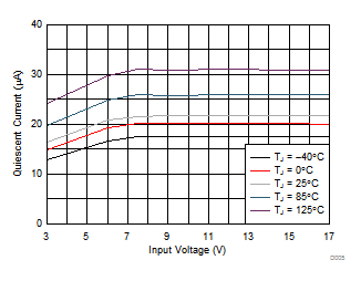
| IQ | Operating quiescent current | EN = High, no load, device not switching TJ = –40 °C to 85 °C |
20 | 35 | µA | ||
| TJ = 125 °C | 58 | ||||||
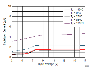
| ISD | Shutdown current into AVIN and PVIN | EN = Low TJ = –40 °C to +85 °C |
2 | 9 | µA | ||
| TJ = 125 °C | 18 | ||||||
| V(UVLO) | Undervoltage lockout threshold | VI falling | 2.6 | 2.7 | 2.8 | V | |
| VI rising | 2.8 | 2.9 | 3 | ||||
| TSD(th) | Thermal shutdown threshold | TJ rising | 160 | °C | |||
| TSD(hys) | Thermal shutdown hysteresis | TJ falling | 20 | ||||
| CONTROL (EN, SS, PG, VIDx, LPM) | |||||||
| VIH | High-level input threshold voltage (EN, VIDx, LPM) | 0.8 | 0.54 | V | |||
| VIL | Low-level input threshold voltage (EN, VIDx, LPM) | 0.47 | 0.3 | V | |||
| R(PD) | Pull down resistor at EN, VIDx, LPM | EN, VIDx, LPM = low | 400 | kΩ | |||
| R(DIS) | Output discharge resistor | EN = Low, VO = 1 V | 20 | kΩ | |||
| Ilkg | Input leakage current at EN, VIDx, LPM | EN, VIDx, LPM = 3.3 V | 0.01 | 1 | µA | ||
| VTH(PG) | Power good threshold DC voltage | VO rising | 736 | 760 | 784 | mV | |
| VO falling | 696 | 720 | 752 | ||||
| VOL(PG) | Power good output low voltage | I(PG) = –2 mA | 0.07 | 0.3 | V | ||
| Ilkg(PG) | Input leakage current at PG | V(PG) = 1.8 V | 1 | 400 | nA | ||
| td(PG) | Power good delay time | PG rising | 140 | µs | |||
| PG falling | 20 | ||||||
| I(SS) | SS pin source current | 2.3 | 2.5 | 2.7 | µA | ||
| POWER SWITCH | |||||||
| rDS(on_H) | High-side MOSFET on-resistance | VI ≥ 6 V | 90 | 170 | mΩ | ||
| rDS(on_L) | Low-side MOSFET on-resistance | VI ≥ 6 V | 40 | 70 | |||
| IL | High-side MOSFET DC current-limit | VI ≥ 5 V, TJ = 25 °C | 3.6 | 4.4 | 5.4 | A | |
| IL(LOW) | High-side MOSFET DC current-limit at low output voltage | VO ≤ 0.3 V | 1.6 | ||||
| OUTPUT | |||||||
| Ilkg(FBS) | Input leakage current at FBS | V(FBS)= 1.1 V | 1 | 100 | nA | ||
| VO(A) | Output voltage accuracy | PWM mode | –1% | 1% | |||
| PSM mode, LPM = High(1) | –1% | 3% | |||||
| ΔVO(ΔIO) | Load regulation(2) | VI = 7.2 V, IO = 0.5 A to 3.2 A | 0.01 | %/A | |||
| ΔVO(ΔVI) | Line regulation(2) | 3 V ≤ VI ≤ 17 V, IO = 1 A | 0.003 | %/V | |||
(1) This is the accuracy provided by the device itself (line and load regulation effects are not included). External components effective value: L = 1 µH and C(OUT) = 47 µF.
(2) Line and load regulation depend on external component selection and layout.
8.5 Typical Characteristics