ZHCSD94C January   2015  – January 2015 TPS62134A , TPS62134B , TPS62134C , TPS62134D

PRODUCTION DATA.  

  1. 特性
  2. 应用
  3. 说明
  4. 典型应用电路
  5. 修订历史记录
  6. Device Comparison Table
  7. Pin Configuration and Functions
  8. Specifications
    1. 8.1 Absolute Maximum Ratings
    2. 8.2 ESD Ratings
    3. 8.3 Recommend Operating Conditions
    4. 8.4 Thermal Information
    5. 8.5 Typical Characteristics
  9. Detailed Description
    1. 9.1 Overview
    2. 9.2 Functional Block Diagram
    3. 9.3 Feature Description
      1. 9.3.1 Enable and Shutdown (EN)
      2. 9.3.2 Undervoltage Lockout (UVLO)
      3. 9.3.3 Soft-Start (SS) Circuitry
      4. 9.3.4 Switch Current-Limit and Short Circuit Protection
      5. 9.3.5 Output Voltage and LPM Logic Selection (VIDx and LPM)
      6. 9.3.6 Power-Good Output (PG)
      7. 9.3.7 Single-Ended Remote Sense (FBS)
      8. 9.3.8 Thermal Shutdown
    4. 9.4 Device Functional Modes
      1. 9.4.1 PWM Operation and Power Save Mode
  10. 10Application and Implementation
    1. 10.1 Application Information
    2. 10.2 Typical Application
      1. 10.2.1 Design Requirements
      2. 10.2.2 Detailed Design Procedure
        1. 10.2.2.1 Output Filter Selection
        2. 10.2.2.2 Inductor Selection
        3. 10.2.2.3 Output Capacitor
        4. 10.2.2.4 Input Capacitor
        5. 10.2.2.5 Soft-Start Capacitor
      3. 10.2.3 Application Curves
  11. 11Power Supply Recommendations
  12. 12Layout
    1. 12.1 Layout Guidelines
    2. 12.2 Layout Example
    3. 12.3 Thermal Considerations
  13. 13器件和文档支持
    1. 13.1 器件支持
      1. 13.1.1 第三方产品免责声明
    2. 13.2 文档支持
      1. 13.2.1 相关文档 
    3. 13.3 相关链接
    4. 13.4 商标
    5. 13.5 静电放电警告
    6. 13.6 术语表
  14. 14机械封装和可订购信息

封装选项

机械数据 (封装 | 引脚)
散热焊盘机械数据 (封装 | 引脚)
订购信息

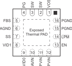
7 Pin Configuration and Functions

RGT Package
16-Pin VQFN With Thermal Pad
Top View
TPS62134A_pinout.gif

Pin Functions

PIN TYPE DESCRIPTION
NO. NAME
1 VOS I Output voltage sense pin and connection for the control loop circuitry. The VOS pin must be connected directly at the output capacitor.
2 SW PWR This pin is a switch node and is connected to the internal MOSFET switches. Connect an inductor between the SW pin and output capacitor.
3
4 PG O Output power-good pin. The PG pin is an open drain and requires a pullup resistor. If this pin is not in use, leave it floating.
5 FBS I Output-voltage feedback pin. This pin is used for a positive remote sense of the load voltage. The FBS pin must be connected close to the load-supply node on the output bus.
6 AGND Analog ground pin. The AGND pin must be connected directly to the exposed thermal pad and common ground plane.
7 SS O Soft-start pin. An external capacitor connected to this pin sets the soft-start time.
8 VID1 I Output-voltage selection pins (VIDx).
9 VID0
10 AVIN I Supply-voltage pin for the internal control circuitry. Connect the AVIN pin to the same source as the PVIN pin.
11 PVIN PWR Supply-voltage pins for the internal power stage.
12
13 EN I Enable and disable input pin. An internal pulldown resistor maintains logic-level low if the pin is floating.
14 LPM I Low-power-mode input pin.
15 PGND Power ground. The PGND pin must be connected directly to the exposed thermal pad and common ground plane.
16
Exposed Thermal Pad The exposed thermal pad must be connected to the AGND (6) pin, PGND (15 and 16) pins, and common ground plane. The thermal pad must be soldered to achieve appropriate power dissipation and mechanical reliability.