ZHCSD94C January 2015 – January 2015 TPS62134A , TPS62134B , TPS62134C , TPS62134D
PRODUCTION DATA.
- 1 特性
- 2 应用
- 3 说明
- 4 典型应用电路
- 5 修订历史记录
- 6 Device Comparison Table
- 7 Pin Configuration and Functions
- 8 Specifications
-
9 Detailed Description
- 9.1 Overview
- 9.2 Functional Block Diagram
- 9.3
Feature Description
- 9.3.1 Enable and Shutdown (EN)
- 9.3.2 Undervoltage Lockout (UVLO)
- 9.3.3 Soft-Start (SS) Circuitry
- 9.3.4 Switch Current-Limit and Short Circuit Protection
- 9.3.5 Output Voltage and LPM Logic Selection (VIDx and LPM)
- 9.3.6 Power-Good Output (PG)
- 9.3.7 Single-Ended Remote Sense (FBS)
- 9.3.8 Thermal Shutdown
- 9.4 Device Functional Modes
- 10Application and Implementation
- 11Power Supply Recommendations
- 12Layout
- 13器件和文档支持
- 14机械封装和可订购信息
12 Layout
12.1 Layout Guidelines
- TI recommends to place all components as close as possible to the device. Ensure that the input capacitor placement is as close as possible to the PVIN and PGND pins of the device.
- The VOS pin is noise sensitive and must be routed short and directly to the output of the output capacitor. This routing minimizes switch node jitter and ensures reliability.
- The direct common-ground connection of the AGND and PGND pins to the exposed thermal pad and the system ground (ground plane) is mandatory. To enhance heat dissipation of the device, the exposed thermal pad should be connected to bottom or internal layer ground planes using vias.
- Use wide and short traces for the main current paths to reduce the parasitic inductance and resistance.
- The capacitor on the SS pin should be placed close to the device and connected directly to those pins and the AGND pin.
- The inductor should be placed close to the SW pins, keeping this area small.
- Finally, the ground of the output capacitor should be located close to the PGND pins of the device.
- See Figure 18 for an example of component placement, routing, and thermal design.
12.2 Layout Example
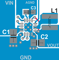 Figure 18. TPS62134x Layout Example
12.3 Thermal Considerations
Implementation of integrated circuits in low-profile and fine-pitch surface-mount packages typically requires special attention to power dissipation. Many system-dependent issues such as thermal coupling, airflow, added heat sinks and convection surfaces, and the presence of other heat-generating components affect the power-dissipation limits of a given component.
The following lists three basic approaches for enhancing thermal performance:
- Improving the power dissipation capability of the PCB design
- Improving the thermal coupling of the component to the PCB by soldering the exposed thermal pad
- Introducing airflow in the system
For more details on how to use the thermal parameters, see the application notes, Thermal Characteristics of Linear and Logic Packages Using JEDEC PCB Designs (SZZA017), and Semiconductor and IC Package Thermal Metrics (SPRA953).