ZHCSD94C January 2015 – January 2015 TPS62134A , TPS62134B , TPS62134C , TPS62134D
PRODUCTION DATA.
- 1 特性
- 2 应用
- 3 说明
- 4 典型应用电路
- 5 修订历史记录
- 6 Device Comparison Table
- 7 Pin Configuration and Functions
- 8 Specifications
-
9 Detailed Description
- 9.1 Overview
- 9.2 Functional Block Diagram
- 9.3
Feature Description
- 9.3.1 Enable and Shutdown (EN)
- 9.3.2 Undervoltage Lockout (UVLO)
- 9.3.3 Soft-Start (SS) Circuitry
- 9.3.4 Switch Current-Limit and Short Circuit Protection
- 9.3.5 Output Voltage and LPM Logic Selection (VIDx and LPM)
- 9.3.6 Power-Good Output (PG)
- 9.3.7 Single-Ended Remote Sense (FBS)
- 9.3.8 Thermal Shutdown
- 9.4 Device Functional Modes
- 10Application and Implementation
- 11Power Supply Recommendations
- 12Layout
- 13器件和文档支持
- 14机械封装和可订购信息
10 Application and Implementation
NOTE
Information in the following applications sections is not part of the TI component specification, and TI does not warrant its accuracy or completeness. TI’s customers are responsible for determining suitability of components for their purposes. Customers should validate and test their design implementation to confirm system functionality.
10.1 Application Information
The TPS62134x family of devices are synchronous step-down converters based on the DCS-Control™ topology. The following section discusses the design of the external components to complete the power-supply design for power rails in the Intel Skylake platform.
10.2 Typical Application
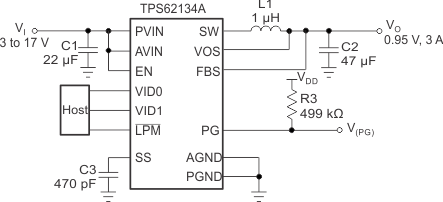 Figure 4. TPS62134A Typical Application
10.2.1 Design Requirements
The design guideline provides component selection to operate the device within the values listed in the Recommend Operating Conditions section. Meanwhile, the design meets the time and slew rate requirements of the Intel Skylake platform for VCC(IO), VCC(PRIM_CORE), VCC(EDRAM), and VCC(EOPIO) rails. Table 3 lists the components used for the curves in the Application Curves section.
Table 3. List of Components
| REFERENCE | DESCRIPTION | MANUFACTURER |
|---|---|---|
| TPS62134x | High efficiency step down converter | TI |
| L1 | Inductor, 1 µH, XFL4020-102ME | Coilcraft |
| C1 | Ceramic capacitor, 22 µF, GRM21BR61E226ME44L | Murata |
| C2 | Ceramic capacitor, 47 µF, GRM21BR60J476ME15L | Murata |
| C3 | Ceramic capactor, 470 pF, GRM188R71H471KA01D | Murata |
| R3 | Resistor, 499 kΩ | Standard |
10.2.2 Detailed Design Procedure
10.2.2.1 Output Filter Selection
The first step of the design procedure is the selection of the output-filter components. The combinations listed in Table 4 are used to simplify the output filter component selection.
Table 4. Recommended LC Output Filter Combinations(1)
| INDUCTOR | OUTPUT CAPACITOR | ||||
|---|---|---|---|---|---|
| 22 µF | 47 µF | 100 µF | 200 µF | 400 µF | |
| 0.47 µH | |||||
| 1 µH | √(2) | √ | √ | ||
| 2.2 µH | |||||
10.2.2.2 Inductor Selection
The inductor selection is affected by several effects such as inductor-ripple current, output-ripple voltage, PWM-to-PSM transition point, and efficiency. In addition, the selected inductor must be rated for appropriate saturation current and DC resistance (DCR). Use Equation 4 to calculate the maximum inductor current under static load conditions.
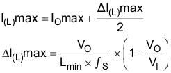
where
- I(L)max is the maximum inductor current
- ΔI(L)max is the maximum peak-to-peak inductor ripple current
- Lmin is the minimum effective inductor value
- ƒS is the actual PWM switching frequency
Calculating the maximum inductor current using the actual operating conditions gives the minimum saturation current. A margin of approximately 20% is recommended to be added. The inductor value also determines the load current at which power save mode is entered:
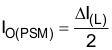
Table 5 lists inductors that are recommended to use with the TPS62134x device.
Table 5. List of Inductors
| TYPE | INDUCTANCE (µH) | CURRENT (A) | DIMENSIONS (L × B × H, mm) | MANUFACTURER |
|---|---|---|---|---|
| XFL4020-102ME | 1 µH | 4.7 | 4 × 4 × 2 | Coilcraft |
| DFE252012F | 1 µH | 5.0 | 2.5 × 2 × 1.2 | Toko |
| DFE201612E | 1 µH | 4.1 | 2 × 1.6 × 1.2 | Toko |
| PISB25201T | 1 µH | 3.9 | 2.5 × 2 × 1 | Cyntec |
| PIME031B | 1 µH | 5.4 | 3.1 × 3.4 × 1.2 | Cyntec |
10.2.2.3 Output Capacitor
The recommended value for the output capacitor is 47 µF. The architecture of the TPS62134x family of devices allows the use of tiny ceramic output capacitors which have low equivalent series resistance (ESR). These capacitors provide low output-voltage ripple and are recommended. Using an X7R or X5R dielectric is recommended to maintain low resistance up to high frequencies and to achieve narrow capacitance variation with temperature. Using a higher value can have some advantages such as smaller voltage ripple and a tighter DC output accuracy in PWM. See Optimizing the TPS62130/40/50/60/70 Output Filter, SLVA463 for additional information.
Note that in power save mode, the output voltage ripple depends on the output capacitance, ESR, and peak inductor current. Using ceramic capacitors provides small ESR and low ripple.
10.2.2.4 Input Capacitor
For most applications, using a capacitor with a value of 22 µF is a recommended. Larger values further reduce input-current ripple. The input capacitor buffers the input voltage for transient events and also decouples the converter from the supply. A ceramic capacitor which has low ESR is recommended for best filtering and should be placed between the PVIN and PGND pins and as close as possible to those pins.
10.2.2.5 Soft-Start Capacitor
A capacitor connected between the SS pin and the AGND pin allows a user programmable startup slope of the output voltage. A constant current source supports 2.5 µA to charge the external capacitance. Use Equation 6 to calculate the capacitor value required for a given soft-start time.
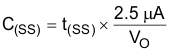
where
- C(SS) is the capacitance (F) required at the SS pin
- t(SS) is the desired soft-start time (s)
Leave the SS pin floating for fastest startup.
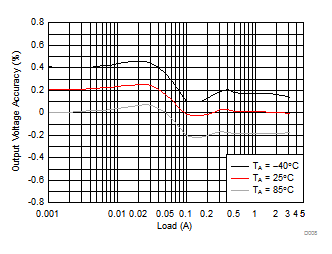
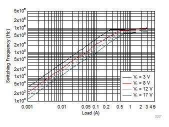
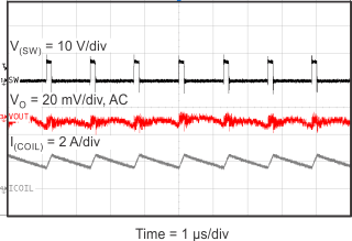
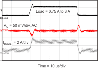
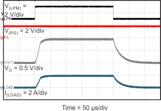
10.2.3 Application Curves
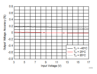
TA = 25°C and VI = 7.2 V, unless otherwise noted.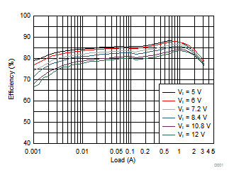
| VO = 0.975 V |
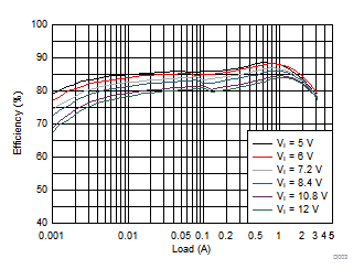
| VO = 1 V |
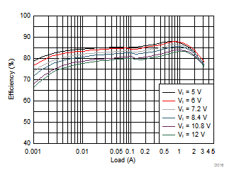
| VO = 0.95 V |
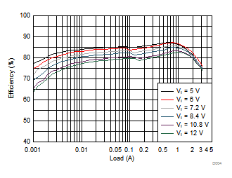
| VO = 0.8 V |
| VO = 0.95 V | VI = 7.2 V | |
| VO = 0.975 V |
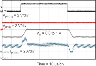
| VO = 0.95 V | IO = 2 A | |
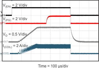
| R(LOAD) = 0.47 Ω | ||||
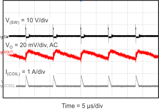
| VO = 0.95 V | IO = 1 A | |
| VO = 0.95 V | IO = 50 mA | |
| VO = 0.95 V | R(LOAD) = 0.47 Ω | |
| R(LOAD) = 0.47 Ω | ||