ZHCSGE4B December 2010 – March 2017 TPS61240-Q1
PRODUCTION DATA.
7 Detailed Description
7.1 Overview
The TPS61240-Q1 boost converter operates with typically a 3.5-MHz fixed-frequency pulse width modulation (PWM) at moderate to heavy load currents. At light load currents, the converter automatically enters Power Save Mode and then operates in pulse frequency modulation (PFM) mode.
During PWM operation the converter uses a unique fast response quasi-constant on-time valley current mode controller scheme, which allows best in class line and load regulation allowing the use of small ceramic input and output capacitors and a small inductor. During shutdown, the load is completely disconnected from the battery.
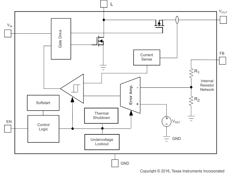
Based on the VIN/VOUT ratio, a simple circuit predicts the required on-time. At the beginning of the switching cycle, the low-side N-MOS switch is turned-on and the inductor current ramps up to a peak current that is defined by the on-time and the inductance. In the second phase, once the peak current is reached, the current comparator trips and the on-timer is reset and this turns off N-MOS switch. Now rectifier switch (P-MOS) is turned on and the inductor current decays to an internally set valley current threshold. Finally, the switching cycle repeats by setting the on timer again and activating the low-side N-MOS switch.
In general, a DC-to-DC step-up converter can only operate in true boost mode, that is, the output is boosted by a certain amount above the input voltage. The TPS61240-Q1 device operates differently as it can smoothly transition in and out of zero duty-cycle operation. Therefore, the output can be kept as close as possible to its regulation limits even though the converter is subject to an input voltage that tends to be excessive.
7.2 Functional Block Diagram

7.3 Feature Description
7.3.1 Current Limit Operation
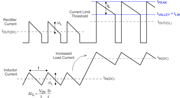
The current limit circuit employs a valley current sensing scheme. Current limit detection occurs during the off time through sensing of the voltage drop across the synchronous rectifier.
During the current limit operation, the output voltage is reduced as the power stage of the device operates in a constant current mode. The maximum continuous output current (IOUT(CL)), before entering current limit operation, can be defined by Equation 1.

Figure 8 illustrates the inductor and rectifier current waveforms during current limit operation. The output current, IOUT, is the average of the rectifier ripple current waveform. When the load current is increased such that the lower peak is above the current limit threshold, the off time is lengthened to allow the current to decrease to this threshold before the next on-time begins (so called frequency fold-back mechanism).
7.3.2 Undervoltage Lockout
The undervoltage lockout circuit prevents the device from malfunctioning at low input voltages and from excessive discharge of the battery. It disables the output stage of the converter once the falling VIN trips the undervoltage lockout threshold VUVLO. The undervoltage lockout threshold VUVLO for falling VIN is 2 V (typical). The device starts operation once the rising VIN trips undervoltage lockout threshold VUVLO again at 2.1 V (typical).
7.3.3 Input Overvoltage Protection
In the event of an overvoltage condition on the input rail, the output voltage will also experience the overvoltage due to being in dropout condition. An input overvoltage protection feature has been implemented into the TPS61240-Q1, which has an input overvoltage threshold of 6 V. Once this level is triggered, the device will go into shutdown mode to protect itself. If the voltage drops to 5.9 V or below, the device will startup once more into normal operation.
7.3.4 Enable
Setting EN pin to high, enables the device. At first, the internal reference is activated and the internal analog circuits are settled. Afterwards, the soft start activates and the output voltage ramps up. The output voltages reach nominal values in typically 250 μs after the device has been enabled.
The EN input can control power sequencing in a system with various DC/DC converters. The EN pin can be connected to the output of another converter, to drive the EN pin high and get a sequencing of supply rails. With EN = GND, the device enters shutdown mode.
7.3.5 Soft Start
The TPS61240-Q1 has an internal soft start circuit that controls the ramp up of the output voltage. Under no load conditions, the output voltage reaches nominal values within tStart of typically 250 μs after EN pin has been pulled to a high level.
This limits the inrush current in the converter during start up and prevents possible input voltage drops when a battery or high impedance power source is used.
During soft start, the switch current limit is reduced to 300 mA until the output voltage reaches VIN. Once the output voltage trips this threshold, the device operates with its nominal current limit ILIMF.
7.3.6 Load Disconnect
Load disconnect electrically removes the output from the input of the power supply when the supply is disabled. This is especially important during shutdown. In shutdown of a boost converter, the load is still connected to the input through the inductor and catch diode. Since the input voltage is still connected to the output, a small current continues to flow, even when the supply is disabled. Even small leakage currents significantly reduce battery life during extended periods of off time.
The benefit of this implemented feature for a system design is that the battery is not depleted during shutdown of the converter. No additional components must be added to the design to make sure that the battery is disconnected from the output of the converter.
7.3.7 Thermal Shutdown
As soon as the junction temperature, TJ, exceeds 140°C (typical) the device goes into thermal shutdown. In this mode, the High Side and Low Side MOSFETs are turned off. When the junction temperature falls below the thermal shutdown hysteresis, the device continues operation.
7.4 Device Functional Modes
7.4.1 Power-Save Mode
The TPS61240-Q1 family of devices integrates a power save mode to improve efficiency at light load. In power save mode, the converter only operates when the output voltage trips below a set threshold voltage. It ramps up the output voltage with several pulses and goes into power save mode once the output voltage exceeds the set threshold voltage.

The PFM mode is left and PWM mode entered in case the output current can not longer be supported in PFM mode.
