ZHCSE52B September 2015 – May 2019 TPS57140-EP
PRODUCTION DATA.
- 1 特性
- 2 应用范围
- 3 说明
- 4 修订历史记录
- 5 Pin Configuration and Functions
- 6 Specifications
-
7 Detailed Description
- 7.1 Overview
- 7.2 Functional Block Diagram
- 7.3
Feature Description
- 7.3.1 Fixed Frequency PWM Control
- 7.3.2 Slope-Compensation Output Current
- 7.3.3 Bootstrap Voltage (Boot)
- 7.3.4 Low-Dropout Operation
- 7.3.5 Error Amplifier
- 7.3.6 Voltage Reference
- 7.3.7 Adjusting the Output Voltage
- 7.3.8 Enable and Adjusting UVLO
- 7.3.9 Slow-Start or Tracking Pin (SS/TR)
- 7.3.10 Overload Recovery Circuit
- 7.3.11 Constant Switching Frequency and Timing Resistor (RT/CLK Pin)
- 7.3.12 Overcurrent Protection and Frequency Shift
- 7.3.13 Selecting the Switching Frequency
- 7.3.14 How to Interface to RT/CLK Pin
- 7.3.15 Power Good (PWRGD Pin)
- 7.3.16 Overvoltage Transient Protection (OVTP)
- 7.3.17 Thermal Shutdown
- 7.3.18 Small-Signal Model for Loop Response
- 7.3.19 Simple Small-Signal Model for Peak-Current-Mode Control
- 7.3.20 Small-Signal Model for Frequency Compensation
- 7.4 Device Functional Modes
-
8 Application and Implementation
- 8.1 Application Information
- 8.2
Typical Application
- 8.2.1 Design Requirements
- 8.2.2
Detailed Design Procedure
- 8.2.2.1 Selecting the Switching Frequency
- 8.2.2.2 Output Inductor Selection (LO)
- 8.2.2.3 Output Capacitor
- 8.2.2.4 Catch Diode
- 8.2.2.5 Input Capacitor
- 8.2.2.6 Slow-Start Capacitor
- 8.2.2.7 Bootstrap Capacitor Selection
- 8.2.2.8 UVLO Set Point
- 8.2.2.9 Output Voltage and Feedback Resistors Selection
- 8.2.2.10 Compensation
- 8.2.3 Application Curves
- 9 Power Supply Recommendations
- 10Layout
- 11器件和文档支持
- 12机械、封装和可订购信息
7.3.13 Selecting the Switching Frequency
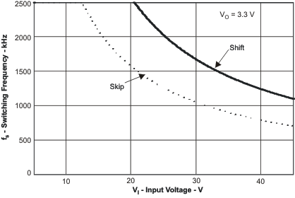
The selected switching frequency should be the lower value of the two equations, Equation 8 and Equation 9. Equation 8 is the maximum switching frequency limitation set by the minimum controllable on-time. Setting the switching frequency above this value causes the regulator to skip switching pulses.
Equation 9 is the maximum switching-frequency limit set by the frequency-shift protection. To have adequate output short-circuit protection at high input voltages, set the switching frequency to be less than the ƒSW(maxshift) frequency. In Equation 9, to calculate the maximum switching frequency, take into account that the output voltage decreases from the nominal voltage to 0 V and that the ƒDIV integer increases from 1 to 8, corresponding to the frequency shift.
In Figure 34, the solid line illustrates a typical safe operating area regarding frequency shift and assumes the output voltage is 0 V, the resistance of the inductor is 0.1 Ω, the FET on-resistance is 0.2 Ω, and the voltage drop of the diode is 0.5 V. The dashed line is the maximum switching frequency to avoid pulse skipping. Enter these equations in a spreadsheet or other software, or use the SwitcherPro design software to determine the switching frequency.


where
- IL = Inductor current
- Rdc = Inductor resistance
- VIN = Maximum input voltage
- VOUT = Output voltage
- VOUTSC = Output voltage during short
- Vd = Diode voltage drop
- rDS(on) = Switch on-resistance
- tON = Controllable on-time
- ƒDIV = Frequency divide (equals 1, 2, 4, or 8)
 Figure 34. Maximum Switching Frequency vs Input Voltage