ZHCSLU7A September 2020 – August 2021 TPS54618C-Q1
PRODUCTION DATA
- 1 特性
- 2 应用
- 3 说明
- 4 Revision History
- 5 Pin Configuration and Functions
- 6 Specifications
-
7 Detailed Description
- 7.1 Overview
- 7.2 Functional Block Diagram
- 7.3
Feature Description
- 7.3.1 Fixed Frequency PWM Control
- 7.3.2 Slope Compensation and Output Current
- 7.3.3 Bootstrap Voltage (Boot) and Low Dropout Operation
- 7.3.4 Error Amplifier
- 7.3.5 Voltage Reference
- 7.3.6 Adjusting the Output Voltage
- 7.3.7 Enable and Adjusting Undervoltage Lockout
- 7.3.8 Soft-Start Pin
- 7.3.9 Sequencing
- 7.3.10 Constant Switching Frequency and Timing Resistor (RT/CLK Pin)
- 7.3.11 Overcurrent Protection
- 7.3.12 Frequency Shift
- 7.3.13 Reverse Overcurrent Protection
- 7.3.14 Synchronize Using the RT/CLK Pin
- 7.3.15 Power Good (PWRGD Pin)
- 7.3.16 Overvoltage Transient Protection
- 7.3.17 Thermal Shutdown
- 7.4 Device Functional Modes
-
8 Application and Implementation
- 8.1 Application Information
- 8.2
Typical Application
- 8.2.1 Design Requirements
- 8.2.2
Detailed Design Procedure
- 8.2.2.1 Step One: Select the Switching Frequency
- 8.2.2.2 Step Two: Select the Output Inductor
- 8.2.2.3 Step Three: Choose the Output Capacitor
- 8.2.2.4 Step Four: Select the Input Capacitor
- 8.2.2.5 Step Five: Choose the Soft-Start Capacitor
- 8.2.2.6 Step Six: Select the Bootstrap Capacitor
- 8.2.2.7 Step Eight: Select Output Voltage and Feedback Resistors
- 8.2.2.8 Step Nine: Select Loop Compensation Components
- 8.2.3 Application Curves
- 9 Power Supply Recommendations
- 10Layout
- 11Device and Documentation Support
- 12Mechanical, Packaging, and Orderable Information
7.4.1 Simple Small Signal Model for Peak Current Mode Control
Figure 7-11 shows an equivalent model for the TPS54618C-Q1 control loop which can be modeled in a circuit simulation program to check frequency response and dynamic load response. The error amplifier is a transconductance amplifier with a gm of 245 μA/V. The error amplifier can be modeled using an ideal voltage controlled current source. The resistor R0 and capacitor Co model the open loop gain and frequency response of the amplifier. The 1-mV AC voltage source between the nodes a and b effectively breaks the control loop for the frequency response measurements. Plotting a/c shows the small signal response of the frequency compensation. Plotting a/b shows the small signal response of the overall loop. The dynamic loop response can be checked by replacing the RL with a current source with the appropriate load step amplitude and step rate in a time domain analysis.
 Figure 7-11 Small Signal Model for Loop Response
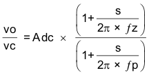
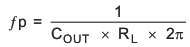
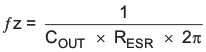
Figure 7-11 is a simple, small-signal model that can be used to understand how to design the frequency compensation. The TPS54618C-Q1 power stage can be approximated to a voltage-controlled current source (duty cycle modulator) supplying current to the output capacitor and load resistor. The control to output transfer function is shown in Equation 11 and consists of a DC gain, one dominant pole, and one ESR zero. The quotient of the change in switch current and the change in COMP pin voltage (node c in Figure 7-11) is the power stage transconductance. The gm for the TPS54618C-Q1 is 25 A/V. The low frequency gain of the power stage frequency response is the product of the transconductance and the load resistance as shown in Equation 12. As the load current increases and decreases, the low frequency gain decreases and increases, respectively. This variation with load can seem problematic at first glance, but the dominant pole moves with load current. The combined effect is highlighted by the dashed line in the right half of Figure 7-13. As the load current decreases, the gain increases and the pole frequency lowers, keeping the 0-dB crossover frequency the same for the varying load conditions which makes it easier to design the frequency compensation.
 Figure 7-12 Small Signal Model for Peak Current Mode Control
 Figure 7-13 Frequency Response Model for Peak Current Mode
Control
Figure 7-13 Frequency Response Model for Peak Current Mode
Control