ZHCSLU7A September 2020 – August 2021 TPS54618C-Q1
PRODUCTION DATA
- 1 特性
- 2 应用
- 3 说明
- 4 Revision History
- 5 Pin Configuration and Functions
- 6 Specifications
-
7 Detailed Description
- 7.1 Overview
- 7.2 Functional Block Diagram
- 7.3
Feature Description
- 7.3.1 Fixed Frequency PWM Control
- 7.3.2 Slope Compensation and Output Current
- 7.3.3 Bootstrap Voltage (Boot) and Low Dropout Operation
- 7.3.4 Error Amplifier
- 7.3.5 Voltage Reference
- 7.3.6 Adjusting the Output Voltage
- 7.3.7 Enable and Adjusting Undervoltage Lockout
- 7.3.8 Soft-Start Pin
- 7.3.9 Sequencing
- 7.3.10 Constant Switching Frequency and Timing Resistor (RT/CLK Pin)
- 7.3.11 Overcurrent Protection
- 7.3.12 Frequency Shift
- 7.3.13 Reverse Overcurrent Protection
- 7.3.14 Synchronize Using the RT/CLK Pin
- 7.3.15 Power Good (PWRGD Pin)
- 7.3.16 Overvoltage Transient Protection
- 7.3.17 Thermal Shutdown
- 7.4 Device Functional Modes
-
8 Application and Implementation
- 8.1 Application Information
- 8.2
Typical Application
- 8.2.1 Design Requirements
- 8.2.2
Detailed Design Procedure
- 8.2.2.1 Step One: Select the Switching Frequency
- 8.2.2.2 Step Two: Select the Output Inductor
- 8.2.2.3 Step Three: Choose the Output Capacitor
- 8.2.2.4 Step Four: Select the Input Capacitor
- 8.2.2.5 Step Five: Choose the Soft-Start Capacitor
- 8.2.2.6 Step Six: Select the Bootstrap Capacitor
- 8.2.2.7 Step Eight: Select Output Voltage and Feedback Resistors
- 8.2.2.8 Step Nine: Select Loop Compensation Components
- 8.2.3 Application Curves
- 9 Power Supply Recommendations
- 10Layout
- 11Device and Documentation Support
- 12Mechanical, Packaging, and Orderable Information
8.2.2.4 Step Four: Select the Input Capacitor
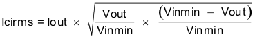
The TPS54618C-Q1 requires a high-quality ceramic, type X5R or X7R, input decoupling capacitor of at least 10 μF of effective capacitance and in some applications, a bulk capacitance. The effective capacitance includes any DC bias effects. The voltage rating of the input capacitor must be greater than the maximum input voltage. The capacitor must also have a ripple current rating greater than the maximum input current ripple of the TPS54618C-Q1. The input ripple current can be calculated using Equation 30.
The value of a ceramic capacitor varies significantly over temperature and the amount of DC bias applied to the capacitor. The capacitance variations due to temperature can be minimized by selecting a dielectric material that is stable over temperature. X5R and X7R ceramic dielectrics are usually selected for power regulator capacitors because they have a high capacitance to volume ratio and are fairly stable over temperature. The output capacitor must also be selected with the DC bias taken into account. The capacitance value of a capacitor decreases as the DC bias across a capacitor increases.
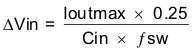
For this example design, a ceramic capacitor with at least a 10-V voltage rating is required to support the maximum input voltage. For this example, two 10-μF and one 0.1-μF 10-V capacitors in parallel have been selected. The input capacitance value determines the input ripple voltage of the regulator. The input voltage ripple can be calculated using Equation 31. Using the design example values (Ioutmax = 6 A, Cin = 20 μF, Fsw = 1 MHz) yields an input voltage ripple of 149 mV and an RMS input ripple current of 2.94 A.