ZHCSLU7A September 2020 – August 2021 TPS54618C-Q1
PRODUCTION DATA
- 1 特性
- 2 应用
- 3 说明
- 4 Revision History
- 5 Pin Configuration and Functions
- 6 Specifications
-
7 Detailed Description
- 7.1 Overview
- 7.2 Functional Block Diagram
- 7.3
Feature Description
- 7.3.1 Fixed Frequency PWM Control
- 7.3.2 Slope Compensation and Output Current
- 7.3.3 Bootstrap Voltage (Boot) and Low Dropout Operation
- 7.3.4 Error Amplifier
- 7.3.5 Voltage Reference
- 7.3.6 Adjusting the Output Voltage
- 7.3.7 Enable and Adjusting Undervoltage Lockout
- 7.3.8 Soft-Start Pin
- 7.3.9 Sequencing
- 7.3.10 Constant Switching Frequency and Timing Resistor (RT/CLK Pin)
- 7.3.11 Overcurrent Protection
- 7.3.12 Frequency Shift
- 7.3.13 Reverse Overcurrent Protection
- 7.3.14 Synchronize Using the RT/CLK Pin
- 7.3.15 Power Good (PWRGD Pin)
- 7.3.16 Overvoltage Transient Protection
- 7.3.17 Thermal Shutdown
- 7.4 Device Functional Modes
-
8 Application and Implementation
- 8.1 Application Information
- 8.2
Typical Application
- 8.2.1 Design Requirements
- 8.2.2
Detailed Design Procedure
- 8.2.2.1 Step One: Select the Switching Frequency
- 8.2.2.2 Step Two: Select the Output Inductor
- 8.2.2.3 Step Three: Choose the Output Capacitor
- 8.2.2.4 Step Four: Select the Input Capacitor
- 8.2.2.5 Step Five: Choose the Soft-Start Capacitor
- 8.2.2.6 Step Six: Select the Bootstrap Capacitor
- 8.2.2.7 Step Eight: Select Output Voltage and Feedback Resistors
- 8.2.2.8 Step Nine: Select Loop Compensation Components
- 8.2.3 Application Curves
- 9 Power Supply Recommendations
- 10Layout
- 11Device and Documentation Support
- 12Mechanical, Packaging, and Orderable Information
7.3.8 Soft-Start Pin
The TPS54618C-Q1 regulates to the lower of the SS/TR pin and the internal reference voltage. A capacitor on the SS/TR pin to ground implements a slow-start time. The TPS54618C-Q1 has an internal pullup current source of 2 μA, which charges the external slow-start capacitor. Equation 4 calculates the required slow-start capacitor value.
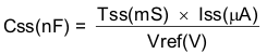
where
- Tss is the desired slow-start time in ms
- Iss is the internal slow-start charging current of 2 μA
- Vref is the internal voltage reference of 0.799 V
If, during normal operation, the VIN goes below UVLO, the EN pin pulls below 1.2 V, or a thermal shutdown event occurs, the TPS54618C-Q1 stops switching. When the VIN goes above UVLO, EN is released or pulled high, or a thermal shutdown is exited, then SS/TR is discharged to below 40 mV before reinitiating a powering-up sequence. The VSENSE voltage follows the SS/TR pin voltage with a 54-mV offset up to 85% of the internal voltage reference. When the SS/TR voltage is greater than 85% on the internal reference voltage, the offset increases as the effective system reference transitions from the SS/TR voltage to the internal voltage reference.