ZHCSJY3D DECEMBER   2003  – June 2019 TPS54110

PRODUCTION DATA.  

  1. 特性
  2. 应用
  3. 说明
    1.     Device Images
  4. 修订历史记录
  5. Device Information
  6. Pin Configuration and Functions
    1.     Pin Functions
  7. Specifications
    1. 7.1 Absolute Maximum Ratings
    2. 7.2 Recommended Operating Conditions
    3. 7.3 Thermal Information
    4. 7.4 Electrical Characteristics
    5. 7.5 Typical Characteristics
  8. Detailed Description
    1. 8.1 Overview
    2. 8.2 Functional Block Diagram
    3. 8.3 Feature Description
      1. 8.3.1 VBIAS Regulator (VBIAS)
      2. 8.3.2 Voltage Reference
      3. 8.3.3 Oscillator and PWM Ramp
      4. 8.3.4 Error Amplifier
      5. 8.3.5 PWM Control
      6. 8.3.6 Dead-Time Control and MOSFET Drivers
      7. 8.3.7 Overcurrent Protection
      8. 8.3.8 Thermal Shutdown
      9. 8.3.9 Power Good (PWRDG)
    4. 8.4 Undervoltage Lockout (UVLO)
    5. 8.5 Slow-Start/Enable (SS/ENA)
  9. Application and Implementation
    1. 9.1 Application Information
    2. 9.2 Typical Applications
      1. 9.2.1 Typical TPS54110 Application
        1. 9.2.1.1 Design Requirements
        2. 9.2.1.2 Detailed Design Procedure
          1. 9.2.1.2.1 Switching Frequency
          2. 9.2.1.2.2 Input Capacitors
          3. 9.2.1.2.3 Output Filter Components
            1. 9.2.1.2.3.1 Inductor Selection
            2. 9.2.1.2.3.2 Capacitor Selection
          4. 9.2.1.2.4 Compensation Components
          5. 9.2.1.2.5 Bias and Bootstrap Capacitors
        3. 9.2.1.3 Application Curves
      2. 9.2.2 Very-Small Form-Factor Application
        1. 9.2.2.1 Design Requirements
        2. 9.2.2.2 Detailed Design Procedure
        3. 9.2.2.3 Application Curves
      3. 9.2.3 Two-Output Sequenced-Startup Application
        1. 9.2.3.1 Design Requirements
        2. 9.2.3.2 Detailed Design Procedure
        3. 9.2.3.3 Application Curve
  10. 10Layout
    1. 10.1 Layout Guidelines
    2. 10.2 Layout Example
    3. 10.3 Layout Considerations For Thermal Performance
    4. 10.4 Grounding and Powerpad Layout
  11. 11器件和文档支持
    1. 11.1 器件支持
      1. 11.1.1 第三方产品免责声明
    2. 11.2 接收文档更新通知
    3. 11.3 社区资源
    4. 11.4 Trademarks
    5. 11.5 Electrostatic Discharge Caution
    6. 11.6 Glossary
  12. 12机械、封装和可订购信息

封装选项

请参考 PDF 数据表获取器件具体的封装图。

机械数据 (封装 | 引脚)
  • PWP|20
散热焊盘机械数据 (封装 | 引脚)
订购信息

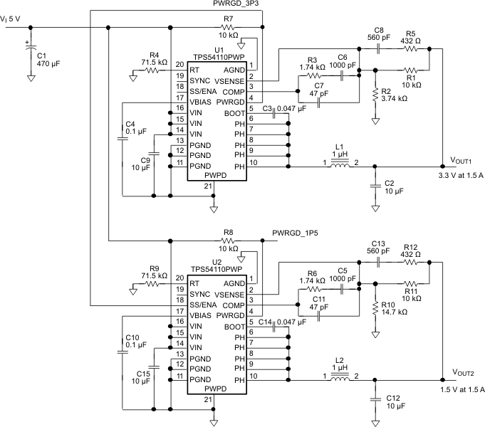
Two-Output Sequenced-Startup Application

In Figure 28, the power-good output of U1 is used as a sequencing signal in a two-output design. Connecting the PWRGD pin of U1 to the SS/ENA pin of U2 causes the 1.5-V output to ramp up after the 3.3-V output is within regulation. Figure 29 shows the start-up waveforms associated with this circuit.

When VIN reaches the UVLO-start threshold, the U1 output ramps up towards the 3.3-V set point. After the output reaches 90 percent of 3.3 V, the U1 asserts the power-good signal driving the U2 SS/ENA input high. The output of U2 then ramps up towards the final output set point of 1.5 V.
TPS54110 sequencing_app_lvs500.gifFigure 28. TPS54110 Sequencing Application Circuit